Table of Contents
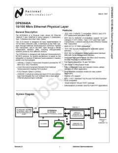
GENERAL DESCRIPTION
FEATURES
4.11 Receive Error Counter Register
4.12 Silicon Revision Register
4.13 PCS Sub-Layer Configuration Register
SYSTEM DIAGRAM
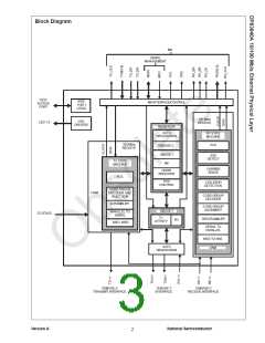
BLOCK DIAGRAM
REVISION HISTORY
TABLE OF CONTENTS
4.14 Loopback, Bypass, and Receive Error
Mask Register
4.15 PHY Address Register
4.16 10BASE-T Status Register
4.17 10BASE-T Configuration Register
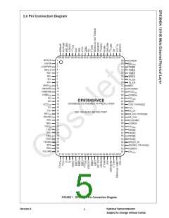
1.0 PIN CONNECTION DIAGRAM
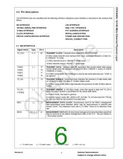
2.0 PIN DESCRIPTION
2.1 MII Interface
5.0 DP83840A APPLICATION
5.1 Typical Board Level Application
5.2 Layout Recommendations
5.3 Plane Partitioning
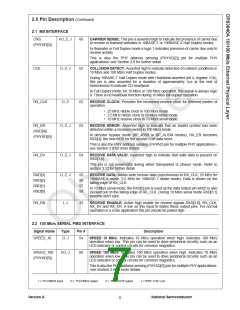
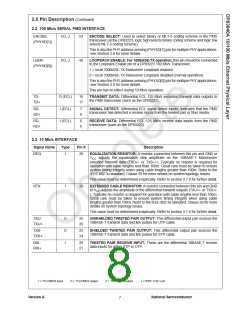
2.2 100 Mb/s Serial PMD Interface
2.3 10 Mb/s Interface
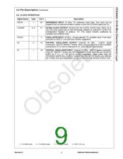
2.4 Clock Interface
5.4 Power and Ground Filtering
2.5 Device Configuration Interface
2.6 LED Interface
6.0 Hardware User Information
6.1 Jabber/Timeout
2.7 IEEE 1149.1 Interface
2.8 PHY Address Interface
2.9 Miscellaneous
6.2 Link Timer
6.3 Link LED, Link Status Bit
6.4 PHYAD[3] and Speed_100
6.5 Collision De-Assertion Time
6.6 Synchronization of Idle
6.7 100 Mb/s Differential Output Voltage
2.10 Power and Ground Pins
2.11 Special Connect Pins
2.12
3.0 FUNCTIONAL DESCRIPTION
3.1 PCS Control
6.8 10Base-T Transmit Differential Output
Impedance
3.2 MII Serial Management Register Access
3.3 100BASE-X Transmitter
3.4 100BASE-X Receiver
6.9 Low Power Mode
6.10 Software Reset
6.11 Receive Error Counter
6.12 Auto-Negotiation Test Compliancy
3.5 Clock Generation Module
3.6 100 Mb/s Clock Recovery Module
3.7 10BASE-T Transceiver Module
3.8 IEEE 1149.1 Controller
3.9 IEEE 802.3u Auto-Negotiation
3.10 Reset Operation
7.0 Software User information
7.1 100Mb/s Full Duplex Log-On
7.2 Auto-Negotiation to Link Sending 100Mb/
s Scrambled Idles
7.3 840A Auto-Negotiating to Legacy Devices
7.4 HBE Disable in 10Mb/s Repeater Mode
7.5 CRS Glitching in 10Mb/s Repeater Mode
3.11 Loopback Operation
3.12 Alternative 100BASE-X Operation
3.13 Low Power Mode
8.0 ELECTRICAL SPECIFICATIONS
8.1 Ratings and Operating Conditions
8.2 DC Specifications
4.0 Registers
4.1 Key to Defaults
4.2 Basic Mode Control Register
4.3 Basic Mode Status Register
4.4 PHY Identifier Register #1
4.5 PHY Identifier Register #2
4.6 Auto-Negotiation Advertisement Register
8.3 Clock Timing
8.4 MII Serial Management AC Timing
8.5 100 Mb/s AC Timing
8.6 10 Mb/s AC Timing
8.7 Fast Link Pulse Timing
8.8 Clock Recovery Module Timing
8.9 Reset Timing
4.7 Auto-Negotiation Link Partner Ability
Register
4.8 Auto-Negotiation Expansion Register
4.9 Disconnect Counter Register
8.10 Loopback Timing
8.11 PHY Isolation Timing
4.10 False Carrier Sense Counter Register
9.0 Package Dimensions
Version A
3
National Semiconductor

 TI [ TEXAS INSTRUMENTS ]