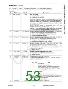
4.0 Registers (Continued)
4.14 LOOPBACK, BYPASS AND RECEIVER ERROR MASK REGISTER (LBREMR)
Address 18h
Bit
Bit Name
Default
Description
15
BAD_SSD_EN
1, RW
BAD SSD Enable:
1 = Enable Bad SSD detection
0 = Disable Bad SSD detection
If Bad SSD is detected, then the DP83840A will assert RX_ER and
present RXD[3:0] = 1110 to the MII for the cycles that correspond to
received 5B symbols until at least two IDLE code groups are detected.
Once at least two IDLE code groups are detected, RX_ER and CRS
become de-asserted.
RX_ER becomes RXD[4] in transparent mode such that
RXD[4:0]=11110 during a Bad SSD event.
When bit 12 of the LBREMR is one (Bypass Align mode), RXD[3:0] and
RX_ER/RXD[4] are not modified regardless of the state of this bit.
14
13
12
BP_4B5B
BP_SCR
(Pin #100), RW BYPASS 4B5B ENCODING AND 5B4B DECODING: The value of the
BP4B5B pin (100) is latched into this bit at power-up/reset.
1 = 4B5B encoder and 5B4B decoder functions bypassed
0 = Normal 4B5B and 5B4B operation
(Pin #1), RW
(Pin #99), RW
BYPASS SCRAMBLER/DESCRAMBLER FUNCTION: The value of
the BPSCR pin (1) is latched into this bit at power-up/reset.
1 = Scrambler and descrambler functions bypassed
0 = Normal scrambler and descrambler operation
BP_ALIGN
BYPASS SYMBOL ALIGNMENT FUNCTION: The value of the
BPALIGN pin (99) is latched into this bit at power-up/reset.
1 = Receive functions (descrambler, symbol alignment and symbol
decoding functions) bypassed. Transmit functions (symbol encoder
and scrambler) bypassed
0 = Normal operation
11
10BT_LPBK
0, RW
10BASE-T ENCODER/DECODER LOOPBACK:
1 = Data loopback in the 10BASE-T ENDEC enabled
0 = Normal Operation
10
Reserved
LB[1:0]
(Pin #49), RW
<00>, RW
RESERVED: Write as 0, read as don't care.
9:8
LOOPBACK CONTROL BITS 1:0: These bits control the 100 Mb/s
loopback function as follows:
LB1 LB0
Mode
0
0
1
0
1
0
Normal Mode
DP83223 Twister Loopback
Remote Loopback--Received data is looped back
to the transmit channel, TD +/-. Received data is
presented to the MII. Data transmitted over the MII
has no effect on TD +/-.
1
1
Reserved
Note that Twister Loopback, like the internal loopback described in the
BMCR bit 14 (address 00h), will produce a “dead time” of 550µs before
any valid data appears at the TD+/- or RXD[3:0] outputs. BMCR bit 14, if
set, take precedence over LB1 and LB0.
Refer to section 3.11 for further detail.
7
Reserved
0, RW
RESERVED: Write as 0, read as don't care.
Version A
National Semiconductor
52

 TI [ TEXAS INSTRUMENTS ]