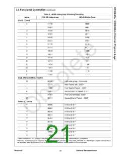
3.0 Functional Description (Continued)
5-bit code-groups. The lower significant 4 bits appear on 3.2.1 Serial Management Access Protocol
TXD[3:0] and RXD[3:0] as normal, and the most significant
The serial control interface consists of two pins,
bits (TXD[4] and RXD[4]) appear on the TX_ER and
Management Data Clock (MDC) and Management Data
RX_ER pins respectively.
Input/Output (MDIO). MDC has a maximum clock rate of
3.1.3.2 10 Mb/s Nibble Mode Operation
2.5 MHz and no minimum rate. The MDIO line is bi-
directional and may be shared by up to 32 devices. The
MDIO frame format is shown in Table I.
For 10 Mb/s nibble mode operation, the MII clock rate is 2.5
MHz. The 100BASE-X bypass functions do not apply to 10
Mb/s operation.
The MDIO pin requires a pull-up resistor (1.5KΩ) which,
during IDLE and Turnaround, will pull MDIO high. Prior to
initiating any transaction, the station management entity
sends a sequence of 32 contiguous logic ones on MDIO to
provide the DP83840A with a sequence that can be used
to establish synchronization. This preamble may be
generated either by driving MDIO high for 32 consecutive
MDC clock cycles, or by simply allowing the MDIO pull-up
resistor to pull the MDIO PHY pin high during which time
32 MDC clock cycles are provided.
3.1.3.3 10 Mb/s Serial Mode Operation
For applications based on serial repeater controllers for 10
Mb/s operation, the DP83840A accepts NRZ serial data on
the TXD[0] input and provides NRZ serial data output on
RXD[0] with a clock rate of 10 MHz. The unused MII inputs
and outputs (TXD[3:1] and RXD[3:1] are ignored during
serial mode. The PCS control signals, CRS, COL, TX_ER,
RX_ER, and RX_DV, continue to function normally.
This mode is selected by setting the 10BT_SER bit in the
10BTSR (bit 9, register address 1Bh). The default value for
this bit is set by the 10BTSER pin 98 at power-up/reset.
The DP83840A waits until it has received this preamble
sequence before responding to any other transaction.
Once the DP83840A serial management port has
initialized no further preamble sequencing is required until
after a Reset/Power-on has occurred.
3.2 MII SERIAL MANAGEMENT REGISTER
ACCESS
The Start code is indicated by a <01> pattern. This assures
the MDIO line transitions from the default idle line state.
The MII specification defines a set of thirty-two 16-bit
status and control registers that are accessible through the
serial management data interface pins MDC and MDIO.
The DP83840A implements all the required MII registers
as well as several optional registers. These registers are
fully described in Section 4. A description of the serial
management access protocol follows.
Turnaround is an idle bit time inserted between the
Register Address field and the Data field. To avoid
contention, no device actively drives the MDIO signal
during the first bit of Turnaround during a read transaction.
The addressed DP83840A drives the MDIO with a zero for
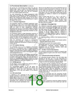
MDC
Z
Z
MDIO
(STA)
Z
Z
Z
MDIO
(PHY)
Z
Z
0 1 1 0 0 1 1 0 0 0 0 0 0 0 0 0 0 1 1 0 0 0 1 0 0 0 0 0 0 0 0
Register Address
(00h = BMCR)
Opcode
(Read)
PHY Address
(PHYAD = 0Ch)
Register Data
Idle
Idle
Start
TA
FIGURE 2. Typical MDC/MDIO Read Operation
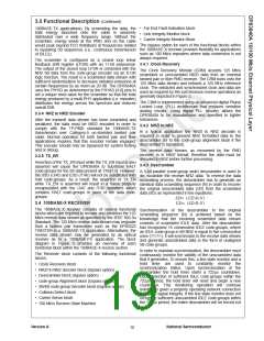
MDC
Z
Z
MDIO
(STA)
Z 0 1 0 1 0 1 1 0 0 0 0 0 0 0 1 0 0 0 0 0 0 0 0 0 0 0 0 0 0 0 0 0
Z
Register Address
(00h = BMCR)
Opcode
(Write)
PHY Address
(PHYAD = 0Ch)
Register Data
Idle
Idle
Start
TA
FIGURE 3. Typical MDC/MDIO Write Operation
Table I.
MII Management
Serial Protocol
<idle><start><op code><device addr> <reg addr><turnaround><data><idle>
Read Operation
Write Operation
<idle><01><10><AAAAA> <RRRRR><Z0><xxxx xxxx xxxx xxxx><idle>
<idle><01><01><AAAAA> <RRRRR><10><xxxx xxxx xxxx xxxx><idle>
Version A
National Semiconductor
16

 TI [ TEXAS INSTRUMENTS ]