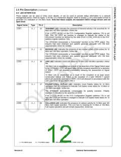
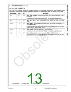
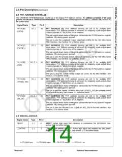
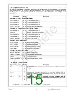
3.0 Functional Description
3.1.1.3 Bypass NRZI Encoder and Decoder
The DP83840A 10/100 Mb/s Ethernet Physical Layer
integrates a 100BASE-X Physical Coding Sub-layer (PCS)
and a complete 10BASE-T module in a single chip. It
provides a standard Media Independent Interface (MII) to
communicate between the Physical Signaling and the
Medium Access Control (MAC) layers for both 100BASE-X
and 10BASE-T operations. It interfaces to a 100 Mb/s
Physical Medium Dependent (PMD) transceiver, such as
the DP83223.
The 100BASE-X NRZI encoder in the transmit channel and
the 100BASE-X NRZI decoder in the receive channel may
be bypassed by setting the NRZI_EN bit in the PCR (bit 15,
register address 17h). The default for this bit is a 1, which
enables the NRZI encoder and decoder. This bypass
option has been included for test purposes only and should
not be selected during normal 100BASE-X operation.
3.1.1.4 Bypass Align
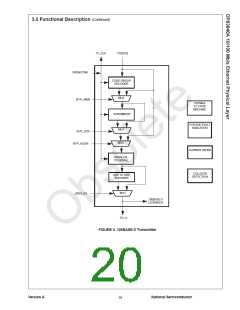
The 100BASE-X section of the device consists of the
following functional blocks:
The 100BASE-X transmit channel operations (4B5B code-
group encoder, scrambler and NRZ to NRZI) and the
100BASE-X receive channel operations (NRZI to NRZ,
descrambler and 4B5B code-group decoding) may all be
bypassed by setting the BP_ALIGN bit in the LBREMR (bit
12, register address 18h). The default value for this bit is
set by the BP_ALIGN signal (pin 99) at power-up/reset.
• Transmitter
• Receiver
• Clock Generation Module (CGM)
• Clock Recovery Module (CRM)
The 10BASE-T section of the device consists primarily of
the 10 Mb/s transceiver module with filters and an ENDEC
module.
The bypass align function is intended for those repeater
applications where none of the transmit and receive
channel operations are required. This mode of operation is
The 100BASE-X and 10BASE-T sections share the referred to as the “Phaser” mode as further defined in
following functional blocks:
section 3.12
• PCS Control
3.1.2 Repeater Mode
• MII Registers
The DP83840A Carrier Sense (CRS) operation depends
on the value of the REPEATER bit in the PCR (bit 12,
register address 17h). When set high, the CRS output (pin
66) is asserted for receive activity only. When set low, the
CRS output is asserted for either receive or transmit
activity. The default value for this bit is set by the
REPEATER pin 47 at power-up/reset.
• IEEE 1149.1 Controller
• IEEE 802.3u Auto-Negotiation
A description of each of these functional blocks follows.
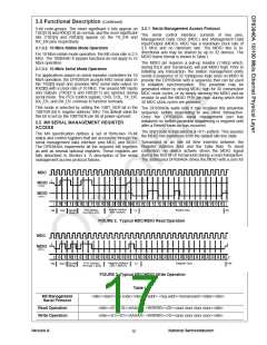
3.1 PCS CONTROL
The IEEE 802.3u 100BASE-X Standard defines the
Physical Coding Sublayer (PCS) as the transmit, receive
and carrier sense functions. These functions within the
DP83840A are controlled via external pins and internal
registers via the MII serial management interface.
When the Repeater mode of operation is selected during
10 Mb/s operation, all functional parameters other than
CRS remain unaffected. CRS will respond only to receive
activity during 10 Mb/s repeater mode.
When the repeater mode of operation is selected during
100 Mb/s operation, there are three parameters that are
directly effected. First, as with 10 Mb/s Repeater operation,
CRS will only respond to receive activity.
3.1.1 100BASE-X Bypass Options
The DP83840A incorporates a highly flexible transmit and
receive channel architecture. Each of the major 100BASE-
X transmit and receive functional blocks of the DP83840A
may be selectively bypassed to provide increased flexibility
for various applications.
Second, in compliance with D5 of the 802.3 standard, the
Carrier Integrity Monitor (CIM) function is automatically
enabled for detection and reporting of bad start of stream
delimiters (whereas in node mode the CIM is disabled).
3.1.1.1 Bypass 4B5B and 5B4B
The 100BASE-X 4B5B code-group encoder in the transmit
channel and the 100BASE-X 5B4B code-group decoder in
the receive channel may be bypassed by setting the
BP_4B5B bit in the LBREMR (bit 14, register address 18h).
The default value for this bit is set by the BP4B5B pin 100
at power-up/reset. This mode of operation is referred to as
the “Transparent” mode as further defined in section 3.12.
Finally, the deassertion of CRS during the reception of a
long Jabber event is effected by the selection of the
repeater mode. If the repeater mode is selected, CRS will
remain asserted even if a long Jabber event (>722us)
occurs. This facilitates proper handling of a jabber event by
the Repeater Controller device. This Jabber related CRS
function can be over-ridden. Refer to section 4.15 (bit 11 of
register 19h) for further detail.
3.1.1.2 Bypass Scrambler and Descrambler
3.1.3 MII Control
The 100BASE-T scrambler in the transmit channel and the
100BASE-T descrambler in the receive channel may be
bypassed by setting the BP_SCR bit in the LBREMR (bit
13, register address 18h). The default value for this bit is
set by the BPSCR signal (pin 1) at power-up/reset. This
bypass option has been included to facilitate 100BASE-FX
operation where data scrambling is not required.
The DP83840A provides three basic MII modes of
operation:
3.1.3.1 100 Mb/s Operation
For 100 Mb/s operation, the MII operates in nibble mode
with a clock rate of 25 MHz. This clock rate is independent
of bypass conditions.
In normal (non-bypassed) operation the MII data at
RXD[3:0] and TXD[3:0] is nibble wide. In bypass mode
(BP_4B5B or BP_ALIGN set) the MII data takes the form of
Version A
National Semiconductor
15

 TI [ TEXAS INSTRUMENTS ]