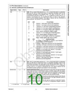
2.0 Pin Description (Continued)
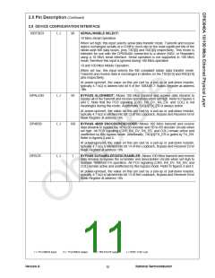
2.8 PHY ADDRESS INTERFACE
The DP83840A PHYAD[4:0] inputs provide up to 32 unique PHY address options. An address selection of all zeros
(00000) will result in a PHY isolation condition. See the Isolate bit description in the BMCR, address 00h, Section 4.2
for further detail.
Signal Name
Type
Pin #
Description
PHYAD[0]
(LBEN)
I/O, J
49
PHY ADDRESS [0]: PHY address sensing pin (bit 0) for multiple PHY
applications. PHY address sensing is achieved by strapping a pull-up/pull-down
resistor (typically 4.7 kΩ) to this pin as required.
The pull-up/pull-down status of this pin is latched into the PHYAD address register
(address 19h) during power up/reset.
This pin is also the Loopback Enable output pin (LBEN) for the 100 Mb/s Serial
PMD Interface. See Section 2.2 for further detail.
PHYAD[1]
(ENCSEL)
I/O, J
I/O, Z, J
I/O, J
53
66
89
63
PHY ADDRESS [1]: PHY address sensing pin (bit 1) for multiple PHY
applications. PHY address sensing is achieved by strapping a pull-up/pull-down
resistor (typically 4.7 kΩ) to this pin as required.
The pull-up/pull-down status of this pin is latched into the PHYAD address register
(address 19h) during power up/reset.
This pin is also the Encode Select output pin (ENCSEL) for the 100 Mb/s Serial
PMD Interface. See Section 2.2 for further detail.
PHYAD[2]
(CRS)
PHY ADDRESS [2]: PHY address sensing pin (bit 2) for multiple PHY
applications. PHY address sensing is achieved by strapping a pull-up/pull-down
resistor (typically 4.7 kΩ) to this pin as required.
The pull-up/pull-down status of this pin is latched into the PHYAD address register
(address 19h) during power up/reset.
This pin is also the Carrier Sense output pin (CRS) for the MII Interface. See
Section 2.1 for further detail.
PHYAD[3]
PHY ADDRESS [3]: PHY address sensing pin (bit 3) for multiple PHY
applications. PHY address sensing is achieved by strapping a pull-up/pull-down
resistor (typically 4.7 kΩ) to this pin as required.
(SPEED_100)
The pull-up/pull-down status of this pin is latched into the PHYAD address register
(address 19h) during power up/reset.
This pin is also the Speed 100 Mb/s output pin (SPEED_100) for optional control
of peripheral circuitry. See Section 2.2 for further detail.
PHYAD[4]
(RX_ER)
I/O, Z, J
PHY ADDRESS [4]: PHY address sensing pin (bit 4) for multiple PHY
applications. PHY address sensing is achieved by strapping a pull-up/pull-down
resistor (typically 4.7 kΩ) to this pin as required.
The pull-up/pull-down status of this pin is latched into the PHYAD address register
(address 19h) during power up/reset.
This pin is also the Receive Error output pin (RX_ER) for the MII Interface. See
Section 2.1 for further detail.
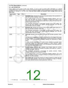
2.9 MISCELLANEOUS
Signal Name
Type
Pin #
Description
RESET
I, J
44
RESET: Active high input that initializes or reinitializes the DP83840A. See
section 3.10 for further detail.
LOWPWR
I, J
3
LOW POWER MODE SELECT: Active high input that enables the low power
mode (100 Mb/s operation only). See section 3.13 for further detail.
I = TTL/CMOS input
O = TTL/CMOS output
Z = TRI-STATE output
J = IEEE 1149.1 pin
Version A
National Semiconductor
13

 TI [ TEXAS INSTRUMENTS ]