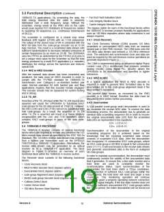
2.10 POWER AND GROUND PINS
The power (VCC) and ground (GND) pins of the DP83840A are grouped in pairs into four categories--TTL/CMOS Input
pairs, TTL/CMOS Output and I/O pairs, 10 Mb/s pairs and 100 Mb/s pairs. This grouping allows for optimizing the layout
and filtering of the power and ground supplies to this device. Refer to section 5.0 for further detail relating to power
supply filtering.
Signal Name
Pin #
Description
GROUP A - TTL/CMOS INPUT SUPPLY PAIRS
IOVCC1, IOGND1
IOVCC2, IOGND2
IOVCC3, IOGND3
PCSVCC, PCSGND
96, 97 TTL Input/Output Supply #1
39, 40 TTL Input/Output Supply #2
51, 52 TTL Input/Output Supply #3
70, 71 Physical Coding Sublayer Supply
GROUP B- TTL/CMOS OUTPUT AND I/O SUPPLY PAIRS
IOVCC4, IOGND4
RCLKGND
59, 60 TTL Input/Output Supply #4
61 Receive Clock Ground, No paired VCC
IOVCC5, IOGND5
IOVCC6, IOGND6
REFVCC, REFGND
68, 69 TTL Input/Output Supply #5
79, 80 TTL Input/Output Supply #6
84, 85 25 MHz Clock Supply
GROUP C- 10 Mb/s SUPPLY PAIRS
RXVCC, RXGND
TDVCC, TDGND
PLLVCC, PLLGND
OVCC, OGND
18, 19 Receive Section Supply
22, 27 Transmit Section Supply
31, 30 Phase Locked Loop Supply
32, 35 Internal Oscillator Supply
GROUP D- 100 Mb/s SUPPLY PAIRS
ANAVCC, ANAGND
CRMVCC, CRMGND
ECLVCC
9, 10 Analog Section Supply
12, 11 Clock Recovery Module Supply
15 ECL Outputs Supply
87, 88 Clock Generator Module Supply
CGMVCC, CGMGND
2.11 SPECIAL CONNECT PINS
Signal Name
Type
Pin #
Description
NC
13
14
83
NO CONNECT: These pins are reserved for future use. Leave them unconnected
(floating).
RES_0
RES_0
4
RESERVED_0: These pins are reserved for future use. This pin must be
connected to ground. For future upgradability, connect this pin to GND via a 0Ω
resistor.
J
45
48
90
RESERVED_0: These pins are reserved for future use. These pins must be
connected to ground. For future upgradability, connect these pins to GND via 0Ω
resistors.
I = TTL/CMOS input
O = TTL/CMOS output
Z = TRI-STATE output
J = IEEE 1149.1 pin
Version A
14
National Semiconductor

 TI [ TEXAS INSTRUMENTS ]