DM385, DM388
www.ti.com
SPRS821D –MARCH 2013–REVISED DECEMBER 2013
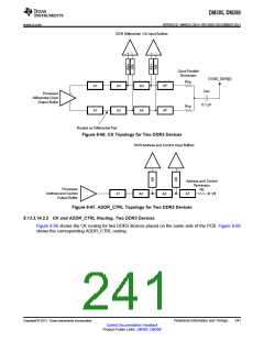
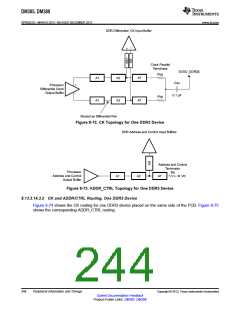
DDR Differential CK Input Buffers
–
–
+
+
Clock Parallel
Terminator
DVDD_DDR[0]
Rcp
A1
A1
A2
A2
A3
A3
AT
Cac
Processor
+
–
Differential Clock
Output Buffer
0.1 µF
Rcp
AT
Routed as Differential Pair
Figure 8-66. CK Topology for Two DDR3 Devices
DDR Address and Control Input Buffers
Address and Control
Terminator
Rtt
Processor
Address and Control
Output Buffer
A1
A2
A3
AT
Vtt
Figure 8-67. ADDR_CTRL Topology for Two DDR3 Devices
8.13.3.14.2.2 CK and ADDR_CTRL Routing, Two DDR3 Devices
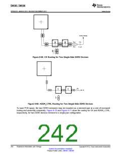
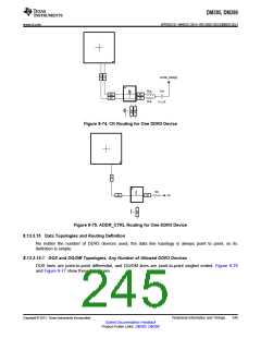
Figure 8-68 shows the CK routing for two DDR3 devices placed on the same side of the PCB. Figure 8-69
shows the corresponding ADDR_CTRL routing.
Copyright © 2013, Texas Instruments Incorporated
Peripheral Information and Timings
241
Submit Documentation Feedback
Product Folder Links: DM385 DM388

 TI [ TEXAS INSTRUMENTS ]