DM385, DM388
SPRS821D –MARCH 2013–REVISED DECEMBER 2013
www.ti.com
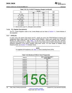
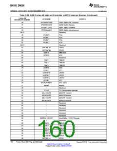
Table 7-23. PLL CLKOUT Frequency Ranges (continued)
OPP100
PLL
UNIT
MIN
10
MAX
400
200
200
400
960
200
200
200
PLL_DDR
PLL_HDVPSS
PLL_AUDIO
PLL_MEDIACTL
PLL_USB
MHz
MHz
MHz
MHz
MHz
MHz
MHz
MHz
10
10
10
10(1)
PLL_VIDEO0
PLL_VIDEO1
PLL_VIDEO2
10
10
10
(1) When the USB is used, PLL_USB must be fixed at 960 MHz.
7.4.6.4 PLL Register Description(s)
The PLL Control Registers reside in the Control Module and are listed in Section 4.1, Control Module of
this datasheet.
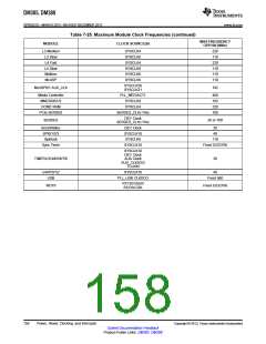
7.4.7 SYSCLKs
In some cases, the system clock inputs and PLL outputs are sent to the PRCM Module for division and
multiplexing before being routed to the various device Modules. These clock outputs from the PRCM
Module are called SYSCLKs. Table Table 7-24 lists the device SYSCLKs along with their maximum
supported clock frequencies. In addition, limits shown in these tables may be further restricted by the clock
frequency limitations of the device modules using these clocks. For more details on Module Clock
frequency limits, see Section 7.4.8 Module Clocks.
NOTE
For supported OPP frequencies, see Table 7-3, Device Operating Points (OPPs).
Table 7-24. Maximum SYSCLK Clock Frequencies
MAX CLOCK FREQUENCY
SYSCLK
OPP100 (MHz)
SYSCLK1
SYSCLK2
SYSCLK3
SYSCLK4
SYSCLK5
SYSCLK6
SYSCLK7
SYSCLK8
SYSCLK9
SYSCLK10
SYSCLK11
SYSCLK12
SYSCLK13
SYSCLK14
SYSCLK15
SYSCLK16
SYSCLK17
RSV
RSV
266
220
RSV
110
RSV
192
RSV
48
RSV
RSV
RSV
27
RSV
27
RSV
156
Power, Reset, Clocking, and Interrupts
Copyright © 2013, Texas Instruments Incorporated
Submit Documentation Feedback
Product Folder Links: DM385 DM388

 TI [ TEXAS INSTRUMENTS ]