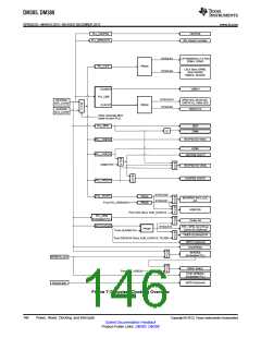
DM385, DM388
www.ti.com
SPRS821D –MARCH 2013–REVISED DECEMBER 2013
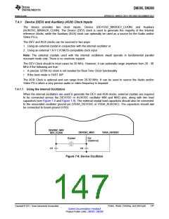
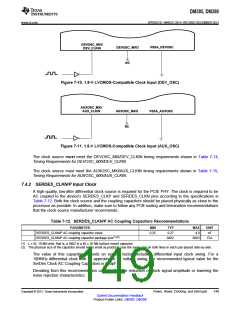
DEVOSC_MXI/
DEV_CLKIN
DEVOSC_MXO
VSSA_DEVOSC
NC
Figure 7-10. 1.8-V LVCMOS-Compatible Clock Input (DEV_OSC)
AUXOSC_MXI/
AUX_CLKIN
AUXOSC_MXO
VSSA_AUXOSC
NC
Figure 7-11. 1.8-V LVCMOS-Compatible Clock Input (AUX_OSC)
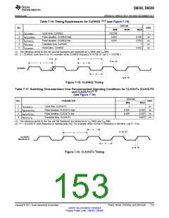
The clock source must meet the DEVOSC_MXI/DEV_CLKIN timing requirements shown in Table 7-14,
Timing Requirements for DEVOSC_MXI/DEV_CLKIN.
The clock source must meet the AUXOSC_MXI/AUX_CLKIN timing requirements shown in Table 7-15,
Timing Requirements for AUXOSC_MXI/AUX_CLKIN.
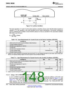
7.4.2 SERDES_CLKN/P Input Clock
A high-quality, low-jitter differential clock source is required for the PCIE PHY. The clock is required to be
AC coupled to the device's SERDES_CLKP and SERDES_CLKN pins according to the specifications in
Table 7-12. Both the clock source and the coupling capacitors should be placed physically as close to the
processor as possible. In addition, make sure to follow any PCB routing and termination recommendations
that the clock source manufacturer recommends.
Table 7-12. SERDES_CLKN/P AC Coupling Capacitors Recommendations
PARAMETER
MIN
TYP
0.27
0402
MAX
4.0
UNIT
nF
SERDES_CLKN/P AC coupling capacitor value
SERDES_CLKN/P AC coupling capacitor package size(1)(2)
0.25
0603
EIA
(1) L x W, 10 Mil units, that is, a 0402 is a 40 x 20 Mil surface mount capacitor.
(2) The physical size of the capacitor should be as small as practical. Use the same size on both lines in each pair placed side-by-side.
The value of this capacitor depends on several factors including differential input clock swing. For a
100MHz differential clock with an approximate 1V voltage swing, the recommended typical value for the
SerDes Clock AC Coupling Capacitors is 270pF.
Deviating from this recommendation can result in the reduction of clock signal amplitude or lowering the
noise rejection characteristics.
Copyright © 2013, Texas Instruments Incorporated
Power, Reset, Clocking, and Interrupts
149
Submit Documentation Feedback
Product Folder Links: DM385 DM388

 TI [ TEXAS INSTRUMENTS ]