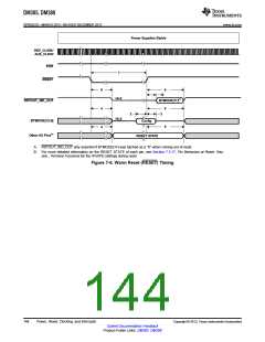
DM385, DM388
SPRS821D –MARCH 2013–REVISED DECEMBER 2013
www.ti.com
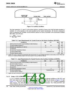
AUXOSC_MXI/
AUX_CLKIN
AUXOSC_MXO
Rd
VSSA_AUXOSC
Crystal
(Optional)
C1
C2
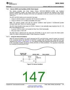
Figure 7-9. Auxiliary Oscillator
The load capacitors, C1 and C2 in the above pictures, should be chosen such that the below equation is
satisfied. CL in the equation is the load specified by the crystal manufacturer. All discrete components
used to implement the oscillator circuit should be placed as close as possible to the associated oscillator
MXI, MXO, and VSS pins.
C C
1
2
C
=
+ Cshunt
L
C
+ C
2
(
)
1
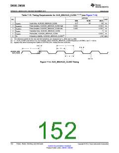
Table 7-10. Input Requirements for Crystal Circuit on the Device Oscillator (DEVOSC)
PARAMETER
MIN
TYP
MAX
4
UNIT
ms
Start-up time (from power up until oscillating at stable frequency)
Crystal Oscillation frequency(1)
Parallel Load Capacitance (C1 and C2)
Crystal ESR
20
12
20
30
24
50
MHz
pF
Ω
Crystal Shunt Capacitance (Cshunt)
Crystal Oscillation Mode
5
pF
Fundamental Only
n/a
ppm
Crystal Frequency stability
±50
(1) 20-MHz DEV clock is required for all bootmodes other than Fast XIP. For more detailed information on boot modes, see the ROM Code
Memory and Peripheral Booting chapter in the device-specific Technical Reference Manual.
Table 7-11. Input Requirements for Crystal Circuit on the Auxiliary Oscillator (AUXOSC)
PARAMETER
Start-up time (from power up until oscillating at stable frequency)
Crystal Oscillation frequency
MIN
TYP
MAX
4
UNIT
ms
20
12
30
24
50
MHz
pF
Parallel Load Capacitance (C1 and C2)
Crystal ESR
Ω
Crystal Shunt Capacitance (Cshunt)
Crystal Oscillation Mode
Crystal Frequency stability(1)
5
pF
Fundamental Only
n/a
ppm
±50
(1) Applies only when sourcing the HDMI or HDVPSS DAC clocks from the AUXOSC
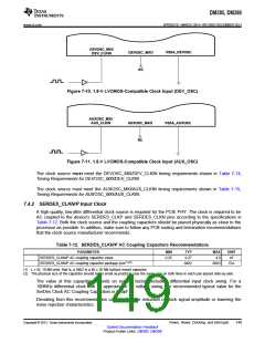
7.4.1.2 Using a 1.8V LVCMOS-Compatible Clock Input
A 1.8-V LVCMOS-Compatible Clock Input can be used instead of the internal oscillators as the DEV and
AUX clock inputs to the system. The external connections to support this are shown in Figure 7-10 and
Figure 7-11. The DEV_CLKIN and AUX_CLKIN pins are connected to the 1.8-V LVCMOS-Compatible
clock sources. The DEV_MXO and AUX_MXO pins are left unconnected. The VSSA_DEVOSC and
VSSA_AUXOSC pins are connected to board ground (VSS).
148
Power, Reset, Clocking, and Interrupts
Copyright © 2013, Texas Instruments Incorporated
Submit Documentation Feedback
Product Folder Links: DM385 DM388

 TI [ TEXAS INSTRUMENTS ]