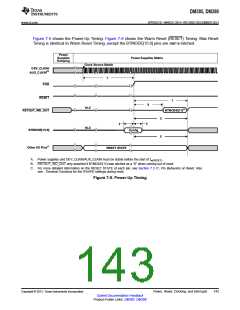
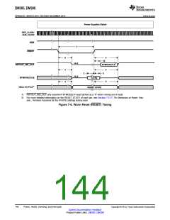
DM385, DM388
www.ti.com
SPRS821D –MARCH 2013–REVISED DECEMBER 2013
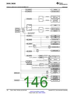
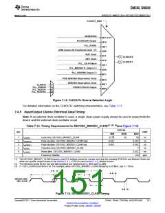
7.4.1 Device (DEV) and Auxiliary (AUX) Clock Inputs
The device provides two clock inputs, Device (DEVOSC_MXI/DEV_CLKIN) and Auxiliary
(AUXOSC_MXI/AUX_CLKIN). The Device (DEV) clock is used to generate the majority of the internal
reference clocks, while the Auxiliary (AUX) clock can optionally be used as a source for the Audio and/or
Video PLLs.
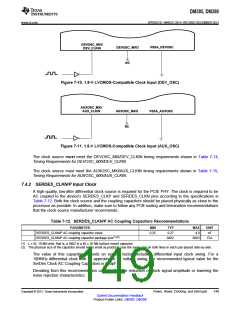
The DEV and AUX clocks can be sourced in two ways:
1. Using an external crystal in conjunction with the internal oscillator or
2. Using an external 1.8-V LVCMOS-compatible clock input
Note: The external crystals used with the internal oscillators must operate in fundamental parallel
resonant mode only. There is no overtone support.
The DEV Clock should in most cases be 20 MHz. However, it can optionally range anywhere from 20 - 30
MHz if the following are true:
•
•
A precise 32768-Hz clock is not needed for Real-Time Clock functionality
If the boot mode is FAST XIP
The AUX Clock is optional and can range from 20-30 MHz. It can be used to source the Audio and/or
Video PLLs when a very precise audio or video frequency is required.
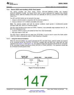
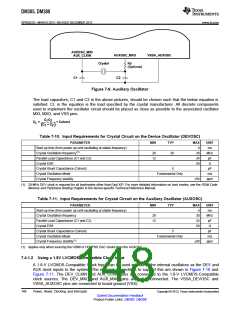
7.4.1.1 Using the Internal Oscillators
When the internal oscillators are used to generate the DEV and AUX clocks, external crystals are required
to be connected across the DEVOSC or AUXOSC oscillator MXI and MXO pins, along with two load
capacitors (see Figure 7-8 and Figure 7-9). The external crystal load capacitors should also be connected
to the associated oscillator ground pin (VSSA_DEVOSC or VSSA_AUXOSC). The capacitors should not
be connected to board ground (VSS).
Figure 7-8. Device Oscillator
Copyright © 2013, Texas Instruments Incorporated
Power, Reset, Clocking, and Interrupts
147
Submit Documentation Feedback
Product Folder Links: DM385 DM388

 TI [ TEXAS INSTRUMENTS ]