DM385, DM388
www.ti.com
SPRS821D –MARCH 2013–REVISED DECEMBER 2013
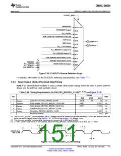
CLKOUT_MUX
RESERVED
RCOSC32K Output
1011-1111
1010
PLL_AUDIO
ARM Cortex-A8 Functional Clock / 16
AUX Clock
1001
1000
0111
CLKOUT0
DEV Clock
0110
CLKOUT1
PLL_L3L4 Output
0101
0100
0011
PLL_MEDIACTL Output / 2
PLL_HDVPSS Output / 2
PCIE SERDES Observation Clock
SERDES Observation Clock
PRCM SYSCLK Output
0010
0001
0000
CLKIN32
PLL_VIDEO0
PLL_HDVICP
PLL_HDVPSS
11
10
01
00
Figure 7-12. CLKOUTx Source Selection Logic
For detailed information on the CLKOUTx switching characteristics, see Table 7-17.
7.4.5 Input/Output Clocks Electrical Data/Timing
Note: If an external clock oscillator is used, a single clean power supply should be used to power both the
device and the external clock oscillator circuit.
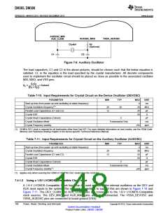
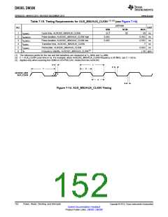
Table 7-14. Timing Requirements for DEVOSC_MXI/DEV_CLKIN(1) (2) (3)(see Figure 7-13)
OPP100
NO.
UNIT
MIN
33.33
0.45C
0.45C
NOM
MAX
50
1
2
3
4
5
tc(DMXI)
tw(DMXIH)
tw(DMXIL)
tt(DMXI)
Cycle time, DEVOSC_MXI/DEV_CLKIN
Pulse duration, DEVOSC_MXI/DEV_CLKIN high
Pulse duration, DEVOSC_MXI/DEV_CLKIN low
Transition time, DEVOSC_MXI/DEV_CLKIN
Period jitter, DEVOSC_MXI/DEV_CLKIN
Frequency Stability
50
ns
ns
0.55C
0.55C
7
ns
ns
tJ(DMXI)
0.02C
±50
ns
ppm
(1) The DEVOSC_MXI/DEV_CLKIN frequency and PLL settings should be chosen such that the resulting SYSCLKs and Module Clocks are
within the specific ranges shown in the Section 7.4.7, SYSCLKs and Section 7.4.8, Module Clocks.
(2) The reference points for the rise and fall transitions are measured at VIL MAX and VIH MIN.
(3) C = DEV_CLKIN cycle time in ns. For example, when DEVOSC_MXI/DEV_CLKIN frequency is 20 MHz, use C = 50 ns.
5
1
4
1
2
DEVOSC_MXI/
DEV_CLKIN
3
4
Figure 7-13. DEV_MXI/DEV_CLKIN Timing
Copyright © 2013, Texas Instruments Incorporated
Power, Reset, Clocking, and Interrupts
151
Submit Documentation Feedback
Product Folder Links: DM385 DM388

 TI [ TEXAS INSTRUMENTS ]