bq76925
www.ti.com
SLUSAM9A –JULY 2011–REVISED JULY 2011
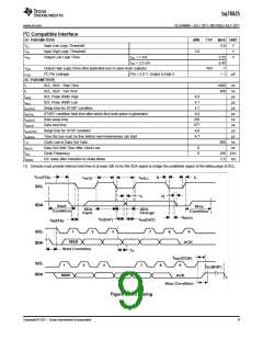
I2C Compatible Interface
DC PARAMETERS
MIN
TYP
MAX UNIT
VIL
Input Low Logic Threshold
Input High Logic Threshold
Output Low Logic Drive
0.6
V
V
V
VIH
VOL
2.8
IOL = 1 mA
0.20
0.40
V
IOL = 2.5 mA
VOH
ILKG
Output High Logic Drive (Not applicable due to open-drain outputs)
I2C Pin Leakage
Pin = 5.0 V, Output in high-Z
N/A
< 1
µA
AC PARAMETERS
tr
SCL, SDAꢀRise Time
1000
300
ns
ns
µs
µs
µs
µs
ns
µs
µs
µs
ns
ns
tf
SCL, SDAꢀFall Time
tw(H)
SCL Pulse Width High
4.0
4.7
4.7
4.0
250
0(1)
4.0
4.7
tw(L)
SCL Pulse Width Low
tsu(STA)
th(STA)
tsu(DAT)
th(DAT)
tsu(STOP)
tsu(BUF)
t V
Setup time for START condition
START condition hold time after which first clock pulse is generated
Data setup time
Data hold time
Setup time for STOP condition
Time the bus must be free before new transmission can start
Clock Low to Data Out Valid
900
th(CH)
fSCL
Data Out Hold Time After Clock Low
Clock Frequency
0
0
100 kHz
2.5 ms
tWAKE
I2C ready after transition to Wake Mode
(1) Devices must provide internal hold time of at least 300 ns for the SDA signal to bridge the undefined region of the falling edge of SCL.
SCL
SDA
SCL
SDA
SCL
SDA
Figure 1. I2C Timing
Copyright © 2011, Texas Instruments Incorporated
9

 TI [ TEXAS INSTRUMENTS ]