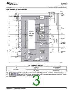
bq76925
www.ti.com
SLUSAM9A –JULY 2011–REVISED JULY 2011
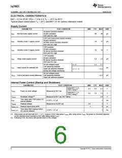
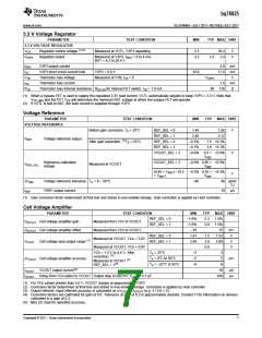
3.3 V Voltage Regulator
PARAMETER
TEST CONDITION
MIN
TYP MAX UNIT
3.3 V VOLTAGE REGULATOR
(1)(2)
VCTL
Regulator control voltage
Regulator output
Measured at VCTL, V3P3 regulating
3.3
3.2
26.4
3.4
V
V
VV3P3
Measured at V3P3, IREG = 0 to 4 mA,
BAT = 4.2 to 26.4 V
3.3
IREG
ISC
V3P3 output current
4.0 mA
17.0 mA
V
V3P3 short circuit current limit
Thermistor bias voltage
Thermistor bias current
V3P3 = 0.0 V
10.0
VTB
ITB
Measured at VTB, ITB = 0
VV3P3
1.0 mA
RTB
Thermistor bias internal resistance RDS,ON for internal FET switch, ITB = 1.0 mA
90 130
Ω
(1) When a bypass FET is used to supply the regulated 3.3V load current, VCTL automatically adjusts to keep V3P3 = 3.3 V. Note that
VCTL,MIN and the FET VGS will determine the minimum BAT voltage at which the bypass FET will operate.
(2) If VCTL is tied to BAT, the load current is supplied through V3P3.
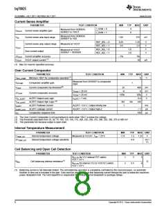
Voltage Reference
PARAMETER
TEST CONDITION
MIN
TYP
MAX UNIT
VOLTAGE REFERENCE
Before gain correction, TA = 25°C
REF_SEL = 0
REF_SEL = 1
REF_SEL = 0
REF_SEL = 1
VCOUT_SEL = 2
1.44
2.88
1.56
3.12
V
VREF
Voltage reference output
After gain correction, (1)TA = 25°C
–0.1%
–0.1%
–0.9%
1.5 +0.1%
3.0 +0.1%
0.5 × +0.9%
V
V
VREF
Reference calibration
voltage
VCOUT_SEL = 3
–0.5% 0.85 × +0.5%
VREF_CAL
Measured at VCOUT
VREF
(0.85 × VREF) – (0.5 –0.3% 0.35 × +0.3%
× VREF VREF
)
∆VREF
Voltage reference tolerance TA = 0 – 50°C
–40
40 ppm/
°C
IREF
VREF output current
10
µA
(1) Gain correction factor determined at final test and stored in non-volatile storage. Gain correction is applied by Host controller.
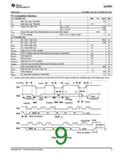
Cell Voltage Amplifier
PARAMETER
TEST CONDITION
REF_SEL = 0
MIN
–1.6%
–1.6%
–16
TYP
MAX UNIT
0.3 1.5%
GVCOUT Cell voltage amplifier gain
OVCOUT Cell voltage amplifier offset
Measured from VCn to VCOUT
Measured from VCn to VCOUT
Measured at VCOUT, VCn = 5.0V
REF_SEL = 1
0.6 1.5%
15
mV
V
REF_SEL = 0
REF_SEL = 1
1.47
1.5
3.0
0.0
1.53
3.06
(1)
VCOUT
Cell voltage amp output range
2.94
V
Measured at VCOUT, VCn = 0.0V
VCn = 1.4 V to 4.4 V, After
V
TA = 25°C
–3
–5
–8
3
5
(2)
correction,
TA = 0°C to 50°C
∆VCOUT Cell voltage amplifier accuracy
mV
(3)
Measured at VCOUT
REF_SEL = 1(4)
TA = –25°C to 85°C
8
IVCOUT
tVCOUT
(1) For VCn values greater than 5.0 V, VCOUT clamps at approximately V3P3.
VCOUT output current(5)
Delay from VCn select to VCOUT Output step of 200 mV. COUT = 0.1 µF
10
100
µA
µs
(2) Correction factor determined at final test and stored in non-volatile storage. Correction is applied by Host controller.
(3) Output referred. Input referred accuracy is calculated as ∆VCOUT / GVCOUT (e.g. 3 / 0.6 = 5).
(4) Correction factors are calibrated for gain of 0.6. Tolerance at gain of 0.3 is approximately doubled. Contact TI for information on devices
calibrated to a gain of 0.3.
(5) Max DC load for specified accuracy.
Copyright © 2011, Texas Instruments Incorporated
7

 TI [ TEXAS INSTRUMENTS ]