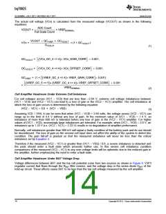
bq76925
www.ti.com
SLUSAM9A –JULY 2011–REVISED JULY 2011
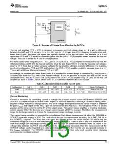
Host ADC Calibration
All analog to digital converters have inherent gain and offset errors which adversely affect measurement
accuracy. Some microcontrollers may be characterized by the manufacturer and shipped with ADC gain and
offset information stored on-chip. It is also possible for such characterization to be done by the end-user on loose
devices prior to PCB assembly, or as a part of the assembled PCB test.
For applications where such ADC characterization is not provided or is not practical, the bq76925 provides a
means for in-situ calibration of the Host ADC. Through setting of the VCOUT_SEL bits in the CELL_CTL register
two scaled versions of the reference voltage, 0.5 × VREF and 0.85 × VREF, can be selected for output on the
VCOUT pin for measurement by the Host ADC. Measuring both scaled voltages enables the Host to do a
two-point calibration of the ADC and compensate for the ADC offset and gain in all subsequent ADC
measurement results as shown in Figure 5.
Note that the calibration accuracy will be limited by the tolerance of the scaled reference voltage output so that
use of this method may not be effective. For these cases, it is recommended to use a higher accuracy source for
the two-point calibration shown in Figure 5.
VOUT
Actual transfer curve:
VADC,ACT = G’ × VIN + VOFFSET
Slope =
Actual gain = G’
Ideal transfer curve:
VADC,IDEAL = VIN
Corrected result:
VADC,COR = (VADC,ACT – VOFFSET) ÷ G’
Slope =
Ideal gain = 1
VOFFSET
VIN
VREF × 0.5
VREF × 0.85
Figure 5. Host ADC Calibration Using VREF
Cell Voltage Monitoring
The cell voltage monitoring circuits include an input level-shifter, multiplexer (MUX) and scaling amplifier. The
Host selects one VCn cell input for measurement by setting the VCOUT_SEL and CELL_SEL bits in the
CELL_CTL register. The scaling factor is set by the REF_SEL bit in the CONFIG_2 register. The selected cell
input is level shifted to VSS reference, scaled by a nominal gain GVCOUT = 0.3 (REF_SEL = 0) or 0.6 (REF_SEL
= 1) and output on the VCOUT pin for measurement by the Host ADC.
Similar to the reference voltage, gain and offset correction factors are determined at final test for each individual
cell input and stored in non-volatile registers VCn_CAL (n = 1-6) and VC_CAL_EXT_m (m = 1-2). These factors
are read by the Host and applied to the ADC voltage measurement results in order to obtain the specified
accuracy.
The cell voltage offset and gain correction factors are stored as 5-bit signed integers in 2’s complement format.
The most significant bits (VCn_OC_4, VCn_GC_4) are stored separately and must be concatenated with the
least significant bits (VCn_OFFSET_CORR, VCn_GAIN_CORR).
The reference voltage offset and gain correction factors are stored respectively as a 6-bit and 5-bit signed integer
in 2’s complement format. As with the cell voltage correction factors, the most significant bits (VREF_OC_5,
VREF_OC_4, VREF_GC_4) are stored separately and must be concatenated with the least significant bits
(VREF_OFFSET_CORR, VREF_GAIN_CORR).
Copyright © 2011, Texas Instruments Incorporated
13

 TI [ TEXAS INSTRUMENTS ]