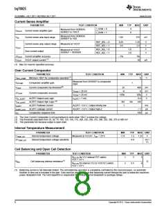
bq76925
SLUSAM9A –JULY 2011–REVISED JULY 2011
www.ti.com
The SLEEP_DIS bit in the POWER_CTL register acts as an override to the sleep function. When SLEEP_DIS is
set to ‘1’, writing the SLEEP bit has no effect (i.e. sleep mode cannot be entered). If SLEEP_DIS is set after
sleep mode has been entered, the device will immediately exit sleep mode. This scenario can arise if
SLEEP_DIS is set after SLEEP is set, but before V3P3 has discharged below a valid operating voltage. This
scenario can also occur if the V3P3 pin is held up by external circuitry and not allowed to fully discharge.
If the over-current alert function is not used, the ALERT pin can function as a dedicated wake-up pin. Otherwise,
the ALERT pin will normally be pulled up to the LDO voltage, so care must be taken in the system design so that
the wake-up signal does not interfere with proper operation of the regulator.
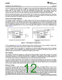
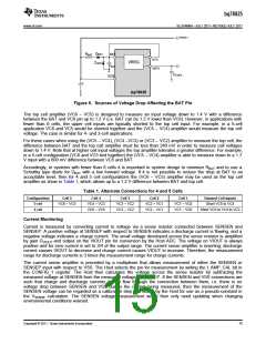
Internal LDO Voltage Regulator
The bq76925 provides a regulated 3.3 V supply voltage on the V3P3 pin for operating the device’s internal logic
and interface circuitry. This regulator may also be used to directly power an external microcontroller or other
external circuitry up to a limit of 4 mA load current. In this configuration, the VCTL pin is tied directly to the BAT
pin. For applications requiring more than 4 mA, an external bypass transistor may be used to supply the load
current. In this configuration the VCTL pin is tied to the gate of the bypass FET. These two configurations are
show in Figure 4.
PACK+
PACK+
3.3 V
RVCTL
BAT
RBAT
CBAT
RBAT
BAT
VCTL
V3P3
VCTL
V3P3
VREG
VREG
CBAT
CV3P3
CV3P3
bq76925
bq76925
a) Regulator load supplied through bq76925
b) Regulator load supplied through external
pass device
Figure 4. LDO Regulator Configurations
For the configuration of Figure 4B), a high gain bypass device should be used to ensure stability. A bipolar PNP
or p-channel FET bypass device may be used. Contact TI for recommendations.
The LDO regulator may be overridden (i.e., back-fed) by an external supply voltage greater than the regulated
voltage on V3P3. In this configuration the bq76925 internal logic and interface circuitry will operate from the
external supply and the internal 3.3 V regulator will supply no load current.
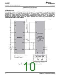
ADC Interface
The bq76925 is designed to interface to a multi-channel analog-to-digital converter (ADC) located in an external
Host controller, such as an MSP430 Microcontroller or equivalent. Three outputs provide voltage, current and
temperature information for measurement by the Host. In addition, the bq76925 includes a low-drift calibrated 1.5
/ 3 V reference that is output on a dedicated pin for use as the reference input to the ADC.
The gain and offset characteristics of the bq76925 are measured during factory test and stored in non-volatile
memory as correction factors. The Host reads these correction factors and applies them to the ADC conversion
results in order to achieve high measurement accuracy. In addition, the precise voltage reference of the bq76925
can be used to calibrate out the gain and offset of the Host ADC.
Reference Voltage
The bq76925 outputs a stable reference voltage for use by the Host ADC. A nominal voltage of 1.5 V or 3 V is
selected via the REF_SEL bit in the CONFIG_2 register. The reference voltage is very stable across
temperature, but the initial voltage may vary by ±4%. The variation from nominal is manifested as a gain error in
the ADC conversion result. To correct for this error, offset and gain correction factors are determined at final test
and stored in the non-volatile registers VREF_CAL and VREF_CAL_EXT. The Host reads the correction factors
and applies them to the nominal reference voltage to arrive at the actual reference voltage as described under
Cell Voltage Monitoring. After gain correction, the tolerance of the reference will be within ±0.1%.
12
Copyright © 2011, Texas Instruments Incorporated

 TI [ TEXAS INSTRUMENTS ]