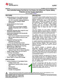
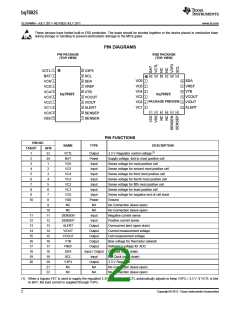
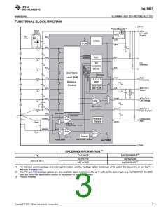
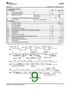
bq76925
www.ti.com
SLUSAM9A –JULY 2011–REVISED JULY 2011
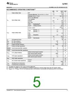
RECOMMENDED OPERATING CONDITIONS(1)
MIN
4.2
TYP
MAX UNIT
Supply voltage range
BAT
26.4
4.4
V
V
Cell input differential, VCn to VCn+1, n = 0 to 5
Cell input, VCn, n = 1 to 6
BAT to VC6 differential
VC0, SENSEN
1.4
4.4 × n
8
V
–8
V
0
V
VIN
Input voltage range
SENSEP
–125
375
5.5
mV
V
SCL, SDA
0
V3P3
Backfeeding(2)
5.5
V
ALERT
Wakeup function
0
0
26.4
V
V3P3 +
0.2
VCOUT, VIOUT
V
REFSEL = 0
1.5
3.0
V
V
VREF
REFSEL = 1
VOUT
Output voltage range
VTB
5.5
V
V3P3
VCTL
ALERT
Regulating
3.3
V
0.8
0
26.4
5.5
50
V
Alert function
V
ICB
Cell balancing current
0
mA
Ω
RBAT
CBAT
RIN
BAT filter resistance
100
10
(3)100
BAT filter capacitance
µF
Ω
External cell input resistance
External cell input capacitance
CIN
0.1
1
10
µF
RSENSEN
RSENSEP
Current sense input filter resistance
Current sense input filter capacitance
1K
Ω
CSENSE
0.1
0
µF
Without external bypass transistor
With external bypass transistor
Without external bypass transistor
With external bypass transistor
RVCTL
VCTL pullup resistance
Ω
200K
4.7
CV3P3
CREF
COUT
V3P3 output capacitance
µF
1.0
VREF output capacitance
ADC channel output capacitance
1.0
0.1
µF
µF
pF
°C
°C
VCOUT
VIOUT
470
–25
–40
2000
85
TOPR
Operating free-air temperature
Functional free-air temperature
TFUNC
100
(1) All voltages are relative to VSS, except “Cell input differential”.
(2) Internal 3.3 V regulator may be overridden (i.e. backfed) by applying an external voltage larger than the regulator voltage.
(3) RIN,MIN = 0.5 × (VCnMAX / 50 mA) if cell balancing used so that maximum recommended cell balancing current is not exceeded
Copyright © 2011, Texas Instruments Incorporated
5

 TI [ TEXAS INSTRUMENTS ]