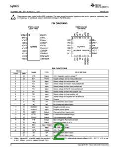
bq76925
www.ti.com
SLUSAM9A –JULY 2011–REVISED JULY 2011
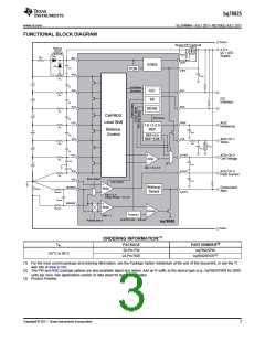
FUNCTIONAL BLOCK DIAGRAM
PACK+
Bypass FET (optional)
Hold-up
circuit
(optiona)l
3.3 V
uC / LED
Supply
RVCTL
DBAT
RBAT
BAT
VCTL
VREG
ZBAT
CBAT
POR
V3P3
VC6
CV3P3
RIN
+
-
CIN
CIN
CIN
CIN
CIN
Cell Select
Bal Select
VC5
VC4
VC3
VC2
VC1
SCL
I2C
EE
RIN
RIN
RIN
RIN
RIN
RIN
+
-
I2C
Interface
SDA
REGS
+
-
Cell MUX
Ref Select
Level Shift
VREF
ADC
Reference
1.5 / 3.0 V
REF
Balance
Control
+
-
CREF
REF×0.5
VTB
REF×0.85
ADC Ch 1
Temp
RTH
RNTC
+
-
CTH
VCOUT
+
Amp
-
ADC Ch 2
Cell Voltage
CIN
+
-
COUT
Gain = 0.3, 0.6
CIN
VC0
VIOUT
ADC Ch 3
Pack Current
Shunt Select
VSS
COUT
Gain Select
+
Amp
SENSEN
Wakeup
Detect
Overcurrent
Alert
RSENSE
RSENSEN
ALERT
-
Gain = 4, 8
Output Range = 1V, 2V
CSENSE
SENSEP
+
Amp
+
RSENSEP
Comp
-
-
ITHRESH
Gain = 1
25,50,75,100,…,400 mV
Polarity Select
bq76925
PACK-
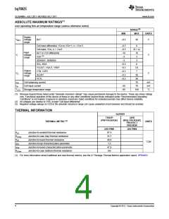
ORDERING INFORMATION(1)
PACKAGE
TA
PART NUMBER(2)
bq76925PW
bq76925RGE(3)
20-Pin PW
–25°C to 85°C
24-Pin RGE
(1) For the most current package and ordering information, see the Package Option Addendum at the end of this document, or see the TI
web site at www.ti.com.
(2) The PW and RGE package options are also available taped and reeled. Add an R suffix to the device type (e.g., bq76925PWR for 2000
units per reel). See applications section of data sheet for layout information.
(3) Product Preview
Copyright © 2011, Texas Instruments Incorporated
3

 TI [ TEXAS INSTRUMENTS ]