bq76925
SLUSAM9A –JULY 2011–REVISED JULY 2011
www.ti.com
These devices have limited built-in ESD protection. The leads should be shorted together or the device placed in conductive foam
during storage or handling to prevent electrostatic damage to the MOS gates.
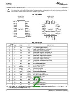
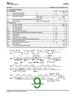
PIN DIAGRAMS
PW PACKAGE
(TOP VIEW)
RGE PACKAGE
(TOP VIEW)
1
2
20
19
18
17
16
15
14
13
12
11
VCTL
BAT
VC6
VC5
VC4
VC3
VC2
VC1
VC0
VSS
V3P3
24 23 22 21 20 19
SCL
3
1
2
3
4
5
6
18
17
16
15
14
13
VC6
VC5
VC4
VC3
VC2
VC1
SDA
SDA
4
VREF
VTB
VREF
VTB
5
bq76925
bq76925
6
VCOUT
VIOUT
ALERT
VCOUT
VIOUT
ALERT
SENSEP
SENSEN
PACKAGE PREVIEW
7
8
9
7
8
9
10 11 12
10
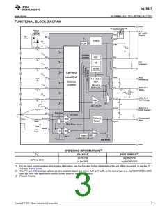
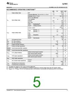
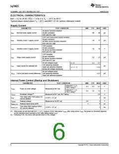
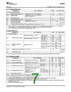
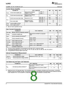
PIN FUNCTIONS
PIN NO.
NAME
TYPE
DESCRIPTION
TSSOP
QFN
23
24
1
1
2
VCTL
BAT
Output
Power
Input
Input
Input
Input
Input
Input
Input
Power
NA
3.3 V Regulator control voltage(1)
Supply voltage, tied to most positive cell
Sense voltage for most positive cell
Sense voltage for second most positive cell
Sense voltage for third most positive cell
Sense voltage for fourth most positive cell
Sense voltage for fifth most positive cell
Sense voltage for least positive cell
Sense voltage for negative end of cell stack
Ground
3
VC6
4
2
VC5
5
3
VC4
6
4
VC3
7
5
VC2
8
6
VC1
9
7
VC0
10
8
VSS
9
NC
No Connection (leave open)
10
11
12
13
14
15
16
17
18
19
20
21
22
NC
NA
No Connection (leave open)
11
12
13
14
15
16
17
18
19
20
SENSEN
SENSEP
ALERT
VIOUT
VCOUT
VTB
Input
Input
Output
Output
Output
Output
Output
Negative current sense
Positive current sense
Overcurrent alert (open drain)
Current measurement voltage
Cell measurement voltage
Bias voltage for thermistor network
Reference voltage for ADC
VREF
SDA
Input / Output I2C Data (open drain)
SCL
Input
Output
NA
I2C Clock (open drain)
V3P3
NC
3.3 V Regulator
No Connection (leave open)
No Connection (leave open)
NC
NA
(1) When a bypass FET is used to supply the regulated 3.3V load current, VCTL automatically adjusts to keep V3P3 = 3.3 V. If VCTL is tied
to BAT, the load current is supplied through V3P3.
2
Copyright © 2011, Texas Instruments Incorporated

 TI [ TEXAS INSTRUMENTS ]