bq76925
SLUSAM9A –JULY 2011–REVISED JULY 2011
www.ti.com
The Host sets GVIOUT by writing the I_GAIN bit in the CONFIG_1 register. The available gains of 4 and 8 enable
operation with a variety of sense resistor values over a broad range of pack currents. The gain may be changed
at any time allowing for dynamic range and resolution adjustment. The input and output ranges of the amplifier
are determined by the value of the REF_SEL bit in the CONFIG_2 register. These values are shown in Table 2.
Because the current amplifier is inverting, the Min column under Output Range corresponds to the Max column
under Input Range. Likewise, the Max column under Output Range corresponds to the Min column under Input
Range.
The actual current is calculated from the measured voltage (VIOUT) as follows. Note that VSENSE is positive when
discharge current is flowing. In keeping with battery pack conventions, the sign of ISENSE is inverted so that
discharge current is negative.
-(VIOUT(SENSEP) - VIOUT(SENSEN))
VSENSE
=
GVIOUT
VSENSE
ISENSE = -
RSENSE
(4)
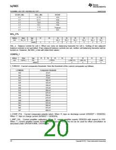
Table 2. Current Amplifier Configurations
Input Range(1) (mV)
Output Range (V)(2)
ISENSE
Resolution
(mA)w/10-bit
ADC(3)
VIOUT (V) at
ISENSE = 0
(typical)
ISENSE Range (A)
at RSENSE = 1
mΩ
REF_SEL
I_GAIN
Gain
Min
Max
Min
Max
0
0
1
1
0
1
0
1
4
8
4
8
1.0
1.0
2.0
2.0
–62.5
–14
187.5
91
0.25
0.27
0.5
1.25
1.11
2.5
–62.5 – 187.5
–14 – 91
366
183
732
366
–125
–62.5
375
–125 – 375
–62.5 – 187.5
187.5
0.5
2.5
(1) SENSEN or SENSEP measured with respect to VSS.
(2) Output range assumes typical value of VIOUT at ISENSE = 0. For non-typical values, the output range will shift accordingly.
(3) Assumes 1 mΩ RSENSE and ADC reference voltage of 1.5 V and 3.0 V when REF_SEL = 0 and 1, respectively.
Over Current Monitoring
The bq76925 also includes a comparator for monitoring the current sense resistor and alerting the Host when the
voltage across the sense resistor exceeds a selected threshold. The available thresholds range from 25 mV to
400 mV and are set by writing the I_THRESH bits in the CONFIG_1 register. Positive (discharge) or negative
(charge) current may be monitored by setting the I_COMP_POL bit in the CONFIG_1 register. By the choice of
sense resistor and threshold a variety of trip points are possible to support a wide range of applications.
The comparator result is driven through the open-drain ALERT output to signal the host when the threshold is
exceeded. This feature can be used to wake up the Host on connection of a load, or to alert the Host to a
potential fault condition. The ALERT pin state is also available by reading the ALERT bit in the STATUS register.
Temperature Monitoring
To enable temperature measurements by the Host, the bq76925 provides the LDO regulator voltage on a
separate output pin (VTB) for biasing an external thermistor network. In order to minimize power consumption,
the Host may switch the VTB output on and off by writing to the VTB_EN bit in the POWER_CTL register. Note
that if the LDO is back-fed by an external source, the VTB bias will be switched to the external source.
In a typical application, the thermistor network will consist of a resistor in series with an NTC thermistor, forming
a resistor divider where the output is proportional to temperature. This output may be measured by the Host ADC
to determine temperature.
Internal Temperature Monitoring
The internal temperature (TINT) of the bq76925 can be measured by setting VCOUT_SEL = ‘01’ and CELL_SEL
= ‘110’ in the CELL_CTL register. In this configuration, a voltage proportional to temperature (VTEMP_INT) is output
on the VCOUT pin. This voltage is related to the internal temperature as follows:
VTEMP_INT(mV) = VTEMP_INT(TINT = 25°C) – TINT(°C) × ΔVTEMP_INT
16
Copyright © 2011, Texas Instruments Incorporated

 TI [ TEXAS INSTRUMENTS ]