bq76925
www.ti.com
SLUSAM9A –JULY 2011–REVISED JULY 2011
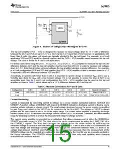
Cell Balancing and Open Cell Detection
The bq76925 integrates cell balancing FETs that are individually controlled by the Host. The balancing method is
resistive bleed balancing, where the balancing current is set by the external cell input resistors. The maximum
allowed balancing current is 50 mA per cell.
The Host may activate one or more cell balancing FETs by writing the BAL_n bits in the BAL_CTL register. To
allow the greatest flexibility, the Host has complete control over the balancing FETs. However, in order to avoid
exceeding the maximum cell input voltage, the bq76925 will prevent two adjacent balancing FETs from being
turned on simultaneously. If two adjacent bits in the balance control register are set to 1, neither balancing
transistor will be turned on. The Host based balancing algorithm must also limit the power dissipation to the
maximum ratings of the device.
In a normal system, closing a cell balancing FET will cause 2 cell voltages to appear across one cell input. This
fact can be utilized to detect a cell sense-line open condition, i.e. a broken wire from the cell sense point to the
bq76925 VCn input. Table 3 shows how this can be accomplished. Note that the normal cell voltage
measurements may represent a saturated or full scale reading. However, these will normally be distinguishable
from the open cell measurement.
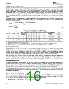
Table 3. Open Cell Detection Method
Method 1
Method 2
Kelvin
input to
test
Result
Result
Turn On
Measure
Turn On
Measure
Normal
Open
CELL2
CELL3
CELL4
CELL5
CELL6
Normal
Open
VC0
VC1
VC2
VC3
VC4
VC5
VC6
BAL_1
BAL_2
BAL_3
BAL_4
BAL_5
CELL2
CELL3
CELL4
CELL5
CELL6
CELL2 + 0.5 × CELL1
CELL3 + 0.5 × CELL2
CELL4 + 0.5 × CELL3
CELL5 + 0.5 × CELL4
CELL6 + 0.5 × CELL5
BAL_2
BAL_3
BAL_4
BAL_5
BAL_6
CELL1
CELL2
CELL3
CELL4
CELL5
CELL1 + 0.5 × CELL2
CELL2 + 0.5 × CELL3
CELL3 + 0.5 × CELL4
CELL4 + 0.5 × CELL5
CELL5 + 0.5 × CELL6
CELL1
CELL2
CELL3
CELL4
CELL5
It should be noted that the cell amplifier headroom limits discussed above apply to the open cell detection
method because by virtue of closing a switch between 2 cell inputs, internally to the device this appears as an
extreme cell imbalance. Therefore, when testing for an open on CELL2 by closing the CELL1 balancing FET, the
CELL2 measurement will be less than the expected normal result due to gain loss caused by the imbalance.
However, the CELL2 measurement will still increase under this condition so that a difference between open (no
change) and normal (measured voltage increases) can be detected.
Host Interface
The Host communicates with the AFE via an I2C interface. A CRC byte may optionally be used to ensure robust
operation. The CRC is calculated over all bytes in the message according to the polynomial x8 + x2 + x + 1.
I2C Addressing
In order to reduce communications overhead, the addressing scheme for the I2C interface combines the slave
device address and device register addresses into a single 7-bit address as shown below.
ADDRESS[6:0] = (I2C_GROUP_ADDR[3:0] << 3) + REG_ADDR[4:0]
The I2C_GROUP_ADDR is a 4-bit value stored in the EEPROM. REG_ADDR is the 5-bit register address being
accessed, and can range from 0x00 – 0x1F. The factory programmed value of the group address is ‘0100’.
Contact TI if an alternative group address is required.
For the default I2C_GROUP_ADDR, the combined address can be formed as shown in Table 4.
Table 4. Combined I2C Address for Default Group
Address
ADDRESS[6:0]
6
5
4:0
0
1
Register address
Copyright © 2011, Texas Instruments Incorporated
17

 TI [ TEXAS INSTRUMENTS ]