AM3359, AM3358, AM3357
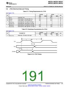
AM3356, AM3354, AM3352
www.ti.com
SPRS717F –OCTOBER 2011–REVISED APRIL 2013
5.8 JTAG Electrical Data and Timing
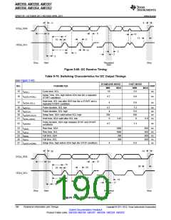
Table 5-71. Timing Requirements for JTAG
(see Figure 5-70)
OPP100
MIN
81.5
32.6
32.6
3
OPP50
UNIT
NO.
MAX
MIN
104.5
41.8
41.8
3
MAX
1
tc(TCK)
1a tw(TCKH)
1b tw(TCKL)
Cycle time, TCK
ns
ns
ns
ns
ns
ns
ns
Pulse duration, TCK high (40% of tc)
Pulse duration, TCK low (40% of tc)
Input setup time, TDI valid to TCK high
Input setup time, TMS valid to TCK high
Input hold time, TDI valid from TCK high
Input hold time, TMS valid from TCK high
tsu(TDI-TCKH)
3
4
tsu(TMS-TCKH)
th(TCKH-TDI)
th(TCKH-TMS)
3
3
8.05
8.05
8.05
8.05
Table 5-72. Switching Characteristics for JTAG
(see Figure 5-70)
OPP100
OPP50
NO.
PARAMETER
UNIT
MIN
MAX
MIN
MAX
2
td(TCKL-TDO)
Delay time, TCK low to TDO valid
3
27.6
4
36.8
ns
1
1a
1b
TCK
TDO
2
3
4
TDI/TMS
Figure 5-70. JTAG Timing
Copyright © 2011–2013, Texas Instruments Incorporated
Peripheral Information and Timings
191
Submit Documentation Feedback
Product Folder Links: AM3359 AM3358 AM3357 AM3356 AM3354 AM3352

 TI [ TEXAS INSTRUMENTS ]