AM3359, AM3358, AM3357
AM3356, AM3354, AM3352
www.ti.com
SPRS717F –OCTOBER 2011–REVISED APRIL 2013
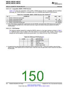
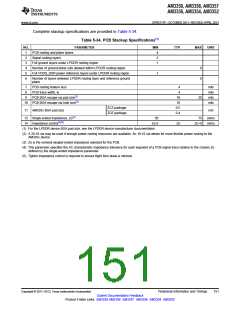
Complete stackup specifications are provided in Table 5-34.
Table 5-34. PCB Stackup Specifications(1)
NO.
1
PARAMETER
MIN
TYP
MAX
UNIT
PCB routing and plane layers
4
2
1
2
Signal routing layers
3
Full ground layers under LPDDR routing region
Number of ground plane cuts allowed within LPDDR routing region
Full VDDS_DDR power reference layers under LPDDR routing region
4
0
0
5
1
6
Number of layers between LPDDR routing layer and reference ground
plane
7
8
9
PCB routing feature size
PCB trace width, w
PCB BGA escape via pad size(2)
4
4
mils
mils
mils
mils
18
10
0.5
0.4
20
10 PCB BGA escape via hole size(2)
ZCZ package
ZCE package
11 AM335x BGA pad size
mm
13 Single-ended impedance, Zo(3)
14 Impedance control(4)(5)
50
75
ohms
ohms
Zo-5
Zo
Zo+5
(1) For the LPDDR device BGA pad size, see the LPDDR device manufacturer documentation.
(2) A 20-10 via may be used if enough power routing resources are available. An 18-10 via allows for more flexible power routing to the
AM335x device.
(3) Zo is the nominal singled-ended impedance selected for the PCB.
(4) This parameter specifies the AC characteristic impedance tolerance for each segment of a PCB signal trace relative to the chosen Zo
defined by the single-ended impedance parameter.
(5) Tighter impedance control is required to ensure flight time skew is minimal.
Copyright © 2011–2013, Texas Instruments Incorporated
Peripheral Information and Timings
151
Submit Documentation Feedback
Product Folder Links: AM3359 AM3358 AM3357 AM3356 AM3354 AM3352

 TI [ TEXAS INSTRUMENTS ]