AM3359, AM3358, AM3357
AM3356, AM3354, AM3352
SPRS717F –OCTOBER 2011–REVISED APRIL 2013
www.ti.com
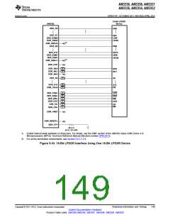
5.6.2.1.2.2 Compatible JEDEC LPDDR Devices
Table 5-32 shows the parameters of the JEDEC LPDDR devices that are compatible with this interface.
Generally, the LPDDR interface is compatible with x16 LPDDR400 speed grade LPDDR devices.
Table 5-32. Compatible JEDEC LPDDR Devices (Per Interface)(1)
NO.
1
PARAMETER
JEDEC LPDDR device speed grade
MIN
LPDDR400
x16
MAX
UNIT
2
JEDEC LPDDR device bit width
JEDEC LPDDR device count
x16
1
Bits
3
Devices
4
JEDEC LPDDR device terminal count
60 Terminals
(1) If the LPDDR interface is operated with a clock frequency less than 200 MHz, lower-speed grade LPDDR devices may be used if the
minimum clock period specified for the LPDDR device is less than or equal to the minimum clock period selected for the AM335x
LPDDR interface.
5.6.2.1.2.3 PCB Stackup
The minimum stackup required for routing the AM335x device is a four-layer stackup as shown in Table 5-
33. Additional layers may be added to the PCB stackup to accommodate other circuitry, enhance signal
integrity and electromagnetic interference performance, or to reduce the size of the PCB footprint.
Table 5-33. Minimum PCB Stackup(1)
LAYER
TYPE
Signal
Plane
Plane
Signal
DESCRIPTION
Top signal routing
Ground
1
2
3
4
Split Power Plane
Bottom signal routing
(1) All signals that have critical signal integrity requirements should be routed first on layer 1. It may not be possible to route all of these
signals on layer 1 which requires some to be routed on layer 4. When this is done, the signal routes on layer 4 should not cross splits in
the power plane.
150
Peripheral Information and Timings
Copyright © 2011–2013, Texas Instruments Incorporated
Submit Documentation Feedback
Product Folder Links: AM3359 AM3358 AM3357 AM3356 AM3354 AM3352

 TI [ TEXAS INSTRUMENTS ]