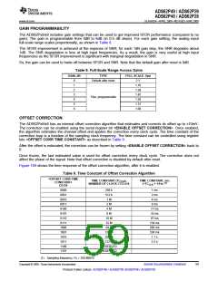
ADS62P49 / ADS62P29
ADS62P48 / ADS62P28
SLAS635A–APRIL 2009–REVISED JUNE 2009............................................................................................................................................................. www.ti.com
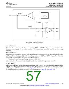
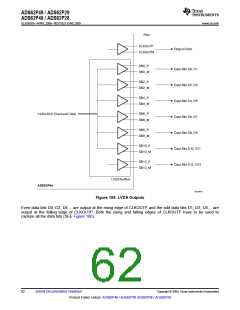
Clock Buffer
Lpkg
» 2 nH
20 W
CLKP
Cbond
» 1 pF
Ceq
Ceq
5 kW
5 kW
Resr
» 100 W
VCM
2 pF
Lpkg
» 2 nH
20 W
CLKM
Cbond
» 1 pF
Resr
» 100 W
Ceq » 1 to 3 pF, Equivalent Input Capacitance of Clock Buffer
S0275-04
Figure 101. Internal Clock Buffer
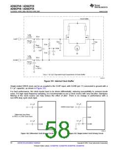
Single-ended CMOS clock can be ac-coupled to the CLKP input, with CLKM (pin 11) connected to ground with a
0.1-µF capacitor, as shown in Figure 103.
For best performance, the clock inputs have to be driven differentially, reducing susceptibility to common-mode
noise. For high input frequency sampling, it is recommended to use a clock source with very low jitter. Bandpass
filtering of the clock source can help reduce the effect of jitter. There is no change in performance with a
non-50% duty cycle clock input.
0.1 mF
0.1 mF
CMOS Clock Input
CLKP
CLKP
Differential Sine-Wave
or PECL or LVDS Clock Input
VCM
0.1 mF
0.1 mF
CLKM
CLKM
S0168-14
S0167-10
Figure 102. Differential Clock Driving Circuit
Figure 103. Single-Ended Clock Driving Circuit
58
Submit Documentation Feedback
Copyright © 2009, Texas Instruments Incorporated
Product Folder Link(s): ADS62P49 / ADS62P29 ADS62P48 / ADS62P28

 TI [ TEXAS INSTRUMENTS ]