ADS62P49 / ADS62P29
ADS62P48 / ADS62P28
SLAS635A–APRIL 2009–REVISED JUNE 2009............................................................................................................................................................. www.ti.com
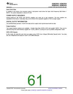
Pins
CLKOUTP
Output Clock
CLKOUTM
DB0_P
Data Bits D0, D1
DB0_M
DB2_P
Data Bits D2, D3
DB2_M
DB4_P
Data Bits D4, D5
DB4_M
DB6_P
DB6_M
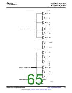
14-Bit ADC Channel-B Data
Data Bits D6, D7
Data Bits D8, D9
Data Bits D10, D11
Data Bits D12, D13
DB8_P
DB8_M
DB10_P
DB10_M
DB12_P
DB12_M
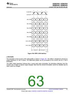
LVDS Buffers
ADS62P4x
S0398-01
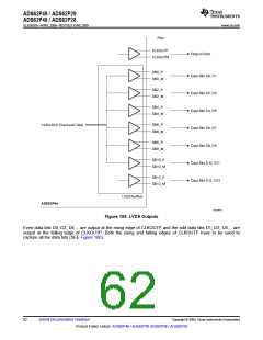
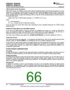
Figure 105. LVDS Outputs
Even data bits D0, D2, D4… are output at the rising edge of CLKOUTP and the odd data bits D1, D3, D5… are
output at the falling edge of CLKOUTP. Both the rising and falling edges of CLKOUTP have to be used to
capture all the data bits (SEE Figure 106).
62
Submit Documentation Feedback
Copyright © 2009, Texas Instruments Incorporated
Product Folder Link(s): ADS62P49 / ADS62P29 ADS62P48 / ADS62P28

 TI [ TEXAS INSTRUMENTS ]