ADS62P49 / ADS62P29
ADS62P48 / ADS62P28
www.ti.com............................................................................................................................................................. SLAS635A–APRIL 2009–REVISED JUNE 2009
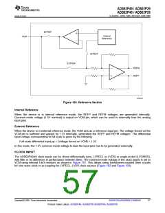
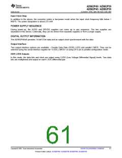
INTREF
Internal
Reference
VCM
INTREF
EXTREF
REFM
REFP
S0165-09
Figure 100. Reference Section
Internal Reference
When the device is in internal reference mode, the REFP and REFM voltages are generated internally.
Common-mode voltage (1.5V nominal) is output on VCM pin, which can be used to externally bias the analog
input pins.
External Reference
When the device is in external reference mode, the VCM acts as a reference input pin. The voltage forced on the
VCM pin is buffered and gained by 1.33 internally, generating the REFP and REFM voltages. The differential
input voltage corresponding to full-scale is given by the following:
Full-scale differential input pp = (Voltage forced on VCM) × 1.33
In this mode, the 1.5V common-mode voltage to bias the input pins has to be generated externally.
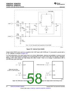
CLOCK INPUT
The ADS62Px9/x8 clock inputs can be driven differentially (sine, LVPECL or LVDS) or single-ended (LVCMOS),
with little or no difference in performance between them. The common-mode voltage of the clock inputs is set to
VCM using internal 5-kΩ resistors as shown in Figure 101. This allows using transformer-coupled drive circuits
for sine wave clock or ac-coupling for LVPECL, LVDS clock sources (Figure 102 and Figure 103).
Copyright © 2009, Texas Instruments Incorporated
Submit Documentation Feedback
57
Product Folder Link(s): ADS62P49 / ADS62P29 ADS62P48 / ADS62P28

 TI [ TEXAS INSTRUMENTS ]