ADS62P49 / ADS62P29
ADS62P48 / ADS62P28
SLAS635A–APRIL 2009–REVISED JUNE 2009............................................................................................................................................................. www.ti.com
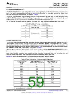
Table 9. Time Constant of Offset Correction Algorithm (continued)
<OFFSET CORR TIME
TIME CONSTANT (TCCLK),
NUMBER OF CLOCK CYCLES
TIME CONSTANT, sec
(=TCCLK × 1/Fs)
CONSTANT>
D3-D0
(1)
1110
1111
RESERVED
RESERVED
8200
Offset Correction Enabled
8195
8190
8185
8180
8175
8170
8165
8160
8155
Output Data With
Offset Corrected
Offset
Correction
Disabled
Output Data
With 34 LSB
Offset
−2
0
2
4
6
8
10 12 14 16 18 20
t − Time − ms
G076
Figure 104. Time Response of Offset Correction
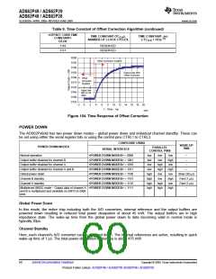
POWER DOWN
The ADS62Px9/x8 has two power down modes – global power down and individual channel standby. These can
be set using either the serial register bits or using the control pins CTRL1 to CTRL3.
CONFIGURE USING
WAKE-UP
POWER DOWN MODES
PARALLEL
TIME
SERIAL INTERFACE
CONTROL PINS
Normal operation
<POWER DOWN MODES> = 0000
<POWER DOWN MODES> = 1001
<POWER DOWN MODES> = 1010
<POWER DOWN MODES> = 1011
<POWER DOWN MODES> = 1100
<POWER DOWN MODES> = 1101
<POWER DOWN MODES> = 1110
low
low
low
low
–
Output buffer disabled for channel B
Output buffer disabled for channel A
Output buffer disabled for channel A and B
Global power down
low
low
high
low
–
high
high
low
–
–
low
high
low
high
high
high
high
Slow (30 µs)
Fast (1 µs)
Fast (1 µs)
–
Channel B standby
low
high
low
Channel A standby
high
high
Multiplexed (MUX) mode – Output data of channel A <POWER DOWN MODES> = 1111
high
and B is multiplexed and available on DA13 to DA0
pins.
Global Power Down
In this mode, the entire chip including both the A/D converters, internal reference and the output buffers are
powered down resulting in reduced total power dissipation of about 45 mW. The output buffers are in high
impedance state. The wake-up time from the global power down to data becoming valid in normal mode is
typically 30µs.
Channel Standby
Here, each channel’s A/D converter can be powered down. The internal references are active, resulting in quick
wake-up time of 1 µs. The total power dissipation in standby is about 475 mW.
60
Submit Documentation Feedback
Copyright © 2009, Texas Instruments Incorporated
Product Folder Link(s): ADS62P49 / ADS62P29 ADS62P48 / ADS62P28

 TI [ TEXAS INSTRUMENTS ]