ADS62P49 / ADS62P29
ADS62P48 / ADS62P28
www.ti.com............................................................................................................................................................. SLAS635A–APRIL 2009–REVISED JUNE 2009
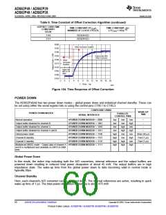
Input Clock Stop
In addition to the above, the converter enters a low-power mode when the input clock frequency falls below 1
MSPS. The power dissipation is about 275 mW.
POWER SUPPLY SEQUENCE
During power-up, the AVDD and DRVDD supplies can come up in any sequence. The two supplies are
separated in the device. Externally, they can be driven from separate supplies or from a single supply.
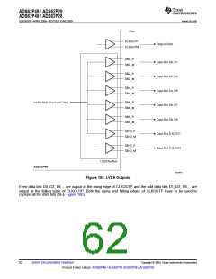
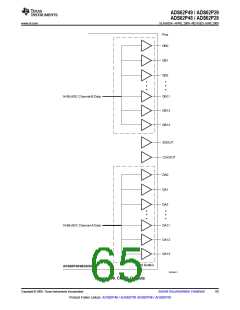
DIGITAL OUTPUT INFORMATION
The ADS62Px9/x8 provides 14-bit/12-bit data and an output clock synchronized with the data.
Output Interface
Two output interface options are available – Double Data Rate (DDR) LVDS and parallel CMOS. They can be
selected using the serial interface register bit <LVDS_CMOS> or using DFS pin in parallel configuration mode.
DDR LVDS Outputs
In this mode, the data bits and clock are output using LVDS (Low Voltage Differential Signal) levels. Two data
bits are multiplexed and output on each LVDS differential pair.
Copyright © 2009, Texas Instruments Incorporated
Submit Documentation Feedback
61
Product Folder Link(s): ADS62P49 / ADS62P29 ADS62P48 / ADS62P28

 TI [ TEXAS INSTRUMENTS ]