ADS62P49 / ADS62P29
ADS62P48 / ADS62P28
www.ti.com............................................................................................................................................................. SLAS635A–APRIL 2009–REVISED JUNE 2009
GAIN PROGRAMMABILITY
The ADS62Px9/x8 includes gain settings that can be used to get improved SFDR performance (compared to no
gain). The gain is programmable from 0dB to 6dB (in 0.5 dB steps). For each gain setting, the analog input
full-scale range scales proportionally, as shown in Table 8.
The SFDR improvement is achieved at the expense of SNR; for each 1dB gain step, the SNR degrades about
1dB. The SNR degradation is less at high input frequencies. As a result, the gain is very useful at high input
frequencies as the SFDR improvement is significant with marginal degradation in SNR.
So, the gain can be used to trade-off between SFDR and SNR. Note that the default gain after reset is 0dB.
Table 8. Full-Scale Range Across Gains
GAIN, dB
TYPE
FULL-SCALE, Vpp
0
1
2
3
4
5
6
Default after reset
2 V
1.78
1.59
1.42
1.26
1.12
1.00
Fine, programmable
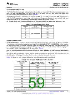
OFFSET CORRECTION
The ADS62Px9/x8 has an internal offset correction algorithm that estimates and corrects dc offset up to ±10mV.
The correction can be enabled using the serial register bit <ENABLE OFFSET CORRECTION>. Once enabled,
the algorithm estimates the channel offset and applies the correction every clock cycle. The time constant of the
correction loop is a function of the sampling clock frequency. The time constant can be controlled using register
bits <OFFSET CORR TIME CONSTANT> as described in Table 9.
After the offset is estimated, the correction can be frozen by setting <ENABLE OFFSET CORRECTION> back to
0.
Once frozen, the last estimated value is used for offset correction every clock cycle. The correction does not
affect the phase of the signal. Note that offset correction is disabled by default after reset.
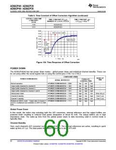
Figure 104 shows the time response of the offset correction algorithm, after it is enabled.
Table 9. Time Constant of Offset Correction Algorithm
<OFFSET CORR TIME
TIME CONSTANT (TCCLK),
NUMBER OF CLOCK CYCLES
TIME CONSTANT, sec
(=TCCLK × 1/Fs)
CONSTANT>
D3-D0
(1)
0000
0001
0010
0011
0100
0101
0110
0111
1000
1001
1010
1011
1100
1101
256 k
512 k
1 ms
2 ms
1 M
4 ms
2 M
8 ms
4 M
17 ms
33 ms
67 ms
134 ms
268 ms
536 ms
1.1 s
8 M
16 M
32 M
64 M
128 M
256 M
512 M
RESERVED
RESERVED
2.2 s
(1) Sampling frequency, Fs = 250 MSPS
Copyright © 2009, Texas Instruments Incorporated
Submit Documentation Feedback
59
Product Folder Link(s): ADS62P49 / ADS62P29 ADS62P48 / ADS62P28

 TI [ TEXAS INSTRUMENTS ]