ADS62P49 / ADS62P29
ADS62P48 / ADS62P28
SLAS635A–APRIL 2009–REVISED JUNE 2009............................................................................................................................................................. www.ti.com
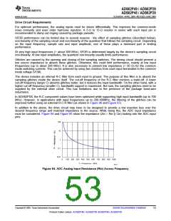
4.5
4.0
3.5
3.0
2.5
2.0
1.5
1.0
0
100 200 300 400 500 600 700 800 900 1000
f − Frequency − MHz
G075
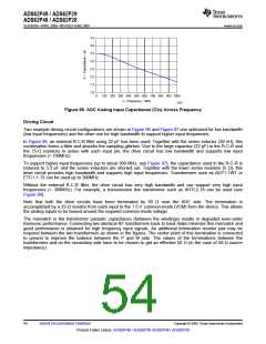
Figure 95. ADC Analog Input Capacitance (Cin) Across Frequency
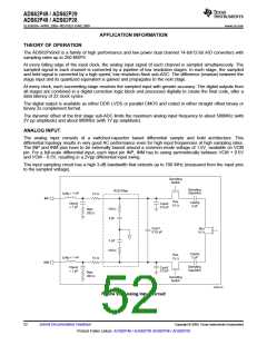
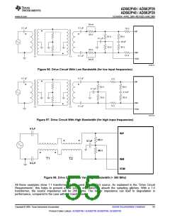
Driving Circuit
Two example driving circuit configurations are shown in Figure 96 and Figure 97 one optimized for low bandwidth
(low input frequencies) and the other one for high bandwidth to support higher input frequencies.
In Figure 96, an external R-C-R filter using 22 pF has been used. Together with the series inductor (39 nH), this
combination forms a filter and absorbs the sampling glitches. Due to the large capacitor (22 pF) in the R-C-R and
the 15-Ω resistors in series with each input pin, the drive circuit has low bandwidth and supports low input
frequencies (< 100MHz).
To support higher input frequencies (up to about 300 MHz, see Figure 97), the capacitance used in the R-C-R is
reduced to 3.3 pF and the series inductors are shorted out. Together with the lower series resistors (5 Ω), this
drive circuit provides high bandwidth and supports high input frequencies. Transformers such as ADT1-1WT or
ETC1-1-13 can be used up to 300MHz.
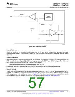
Without the external R-C-R filter, the drive circuit has very high bandwidth and can support very high input
frequencies (> 300MHz). For example, a transmission line transformer such as ADTL2-18 can be used (see
Figure 98).
Note that both the drive circuits have been terminated by 50 Ω near the ADC side. The termination is
accomplished by a 25-Ω resistor from each input to the 1.5-V common-mode (VCM) from the device. This allows
the analog inputs to be biased around the required common-mode voltage.
The mismatch in the transformer parasitic capacitance (between the windings) results in degraded even-order
harmonic performance. Connecting two identical RF transformers back to back helps minimize this mismatch and
good performance is obtained for high frequency input signals. An additional termination resistor pair may be
required between the two transformers as shown in the figures. The center point of this termination is connected
to ground to improve the balance between the P and M side. The values of the terminations between the
transformers and on the secondary side have to be chosen to get an effective 50 Ω (in the case of 50-Ω source
impedance).
54
Submit Documentation Feedback
Copyright © 2009, Texas Instruments Incorporated
Product Folder Link(s): ADS62P49 / ADS62P29 ADS62P48 / ADS62P28

 TI [ TEXAS INSTRUMENTS ]