ADS131M04-Q1
ZHCSOL7A –MARCH 2022 –REVISED AUGUST 2022
www.ti.com.cn
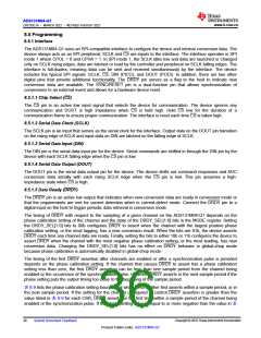
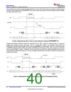
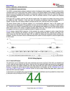
图8-20 depicts an example of how to collect data after a period of the ADC running, but where no data are being
retrieved. In this instance, the SYNC/RESET pin is used to clear the internal FIFOs and realign the ADS131M04-
Q1 output data with the host.
Time where data is
not being read
DRDY
SYNC / RESET
SYNC Pulse
CS
SCLK
Hi-Z
DOUT
Data
Data
CRC
Status
Data
CRC
图8-20. Collecting Data After a Pause in Data Collection Using the SYNC/RESET Pin
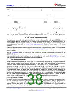
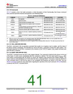
Another functionally equivalent method for clearing the FIFO after a pause in collecting data is to begin by
reading two samples in quick succession. 图 8-21 depicts this method. This example shows when the
DRDY_FMT bit in the MODE register is set to 0b indicating DRDY is a level output. There is a very narrow pulse
on DRDY immediately after the first set of data are shifted out of the device. This pulse may be too narrow for
some microcontrollers to detect. Therefore, do not rely upon this pulse but instead immediately read out the
second data set after the first data set. The host operates synchronous to the device after the second word is
read from the device.
Time where data is
not being read
Narrow DRDY Pulse
DRDY
CS
SCLK
Hi-Z
DOUT
Data
Data
CRC
Status
Data
CRC
Status
Data
CRC
Data is read a
second time
图8-21. Collecting Data After a Pause in Data Collection by Reading Data Twice
Copyright © 2022 Texas Instruments Incorporated
40
Submit Document Feedback
Product Folder Links: ADS131M04-Q1

 TI [ TEXAS INSTRUMENTS ]