ADS131M04-Q1
ZHCSOL7A –MARCH 2022 –REVISED AUGUST 2022
www.ti.com.cn
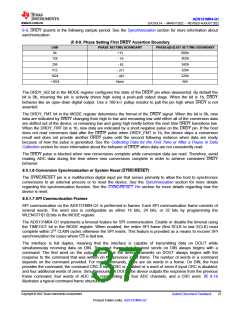
8-9, DRDY asserts in the following sample period. See the Synchronization section for more information about
synchronization.
表8-9. Phase Setting First DRDY Assertion Boundary
OSR
64
PHASE SETTING BOUNDARY
PHASEn[9:0] BIT SETTING BOUNDARY
+13
–19
00Dh
3EDh
128
256
512
3ADh
32Dh
22Dh
N/A
–83
–211
–467
None
1024
>1024
The DRDY_HIZ bit in the MODE register configures the state of the DRDY pin when deasserted. By default the
bit is 0b, meaning the pin is actively driven high using a push-pull output stage. When the bit is 1b, DRDY
behaves like an open-drain digital output. Use a 100-kΩ pullup resistor to pull the pin high when DRDY is not
asserted.
The DRDY_FMT bit in the MODE register determines the format of the DRDY signal. When the bit is 0b, new
data are indicated by DRDY changing from high to low and remaining low until either all of the conversion data
are shifted out of the device, or remaining low and going high briefly before the next time DRDY transitions low.
When the DRDY_FMT bit is 1b, new data are indicated by a short negative pulse on the DRDY pin. If the host
does not read conversion data after the DRDY pulse when DRDY_FMT is 1b, the device skips a conversion
result and does not provide another DRDY pulse until the second following instance when data are ready
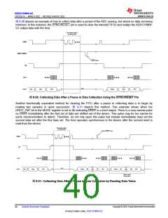
because of how the pulse is generated. See the Collecting Data for the First Time or After a Pause in Data
Collection section for more information about the behavior of DRDY when data are not consistently read.
The DRDY pulse is blocked when new conversions complete while conversion data are read. Therefore, avoid
reading ADC data during the time where new conversions complete in order to achieve consistent DRDY
behavior.
8.5.1.6 Conversion Synchronization or System Reset (SYNC/RESET)
The SYNC/RESET pin is a multifunction digital input pin that serves primarily to allow the host to synchronize
conversions to an external process or to reset the device. See the Synchronization section for more details
regarding the synchronization function. See the SYNC/RESET Pin section for more details regarding how the
device is reset.
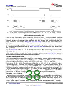
8.5.1.7 SPI Communication Frames
SPI communication on the ADS131M04-Q1 is performed in frames. Each SPI communication frame consists of
several words. The word size is configurable as either 16 bits, 24 bits, or 32 bits by programming the
WLENGTH[1:0] bits in the MODE register.
The ADS131M04-Q1 implements a timeout feature for SPI communication. Enable or disable the timeout using
the TIMEOUT bit in the MODE register. When enabled, the entire SPI frame (first SCLK to last SCLK) must
complete within 215 CLKIN cycles otherwise the SPI resets. This feature is provided as a means to recover SPI
synchronization for cases where CS is tied low.
The interface is full duplex, meaning that the interface is capable of transmitting data on DOUT while
simultaneously receiving data on DIN. The input frame that the host sends on DIN always begins with a
command. The first word on the output frame that the device transmits on DOUT always begins with the
response to the command that was written on the previous input frame. The number of words in a command
depends on the command provided. For most commands, there are six words in a frame. On DIN, the host
provides the command, the command CRC if input CRC is enabled or a word of zeros if input CRC is disabled,
and four additional words of zeros. Simultaneously on DOUT, the device outputs the response from the previous
frame command, four words of ADC data representing the four ADC channels, and a CRC word. 图 8-18
illustrates a typical command frame structure.
Copyright © 2022 Texas Instruments Incorporated
Submit Document Feedback
37
Product Folder Links: ADS131M04-Q1

 TI [ TEXAS INSTRUMENTS ]