ADS131M04-Q1
ZHCSOL7A –MARCH 2022 –REVISED AUGUST 2022
www.ti.com.cn
Conversion data are 24 bits. The data LSBs are truncated when the device operates with a 16-bit word size. The
LSBs are zero padded or the MSBs sign extended when operating with a 32-bit word size depending on the
setting of the WLENGTH[1:0] bits in the MODE register.
Data are given in binary two's complement format. Use 方程式10 to calculate the size of one code (LSB).
1 LSB = (2.4 / Gain) / 224 = +FSR / 223
(10)
A positive full-scale input VIN ≥+FSR –1 LSB = 1.2 / Gain –1 LSB produces an output code of 7FFFFFh and
a negative full-scale input (VIN ≤ –FSR = –1.2 / Gain) produces an output code of 800000h. The output clips
at these codes for signals that exceed full-scale.
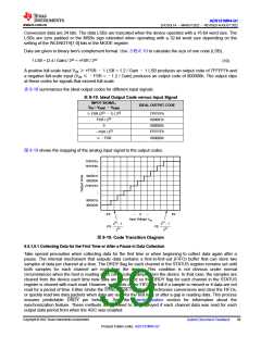
表8-10 summarizes the ideal output codes for different input signals.
表8-10. Ideal Output Code versus Input Signal
INPUT SIGNAL,
IDEAL OUTPUT CODE
VIN = VAINP –VAINN
≥FSR (223 –1) / 223
FSR / 223
7FFFFFh
000001h
000000h
FFFFFFh
800000h
0
–FSR / 223
≤–FSR
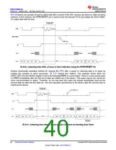
图8-19 shows the mapping of the analog input signal to the output codes.
7FFFFFh
7FFFFEh
000001h
000000h
FFFFFFh
800001h
800000h
¼
¼
-FS
-FS
0
FS
Input Voltage VIN
223 - 1
223 - 1
FS
223
223
图8-19. Code Transition Diagram
8.5.1.9.1 Collecting Data for the First Time or After a Pause in Data Collection
Take special precaution when collecting data for the first time or when beginning to collect data again after a
pause. The internal mechanism that outputs data contains a first-in-first-out (FIFO) buffer that can store two
samples of data per channel at a time. The DRDY flag for each channel in the STATUS register remains set until
both samples for each channel are read from the device. This condition is not obvious under normal
circumstances when the host is reading each consecutive sample from the device. In that case, the samples are
cleared from the device each time new data are generated so the DRDY flag for each channel in the STATUS
register is cleared with each read. However, both slots of the FIFO are full if a sample is missed or if data are not
read for a period of time. Either strobe the SYNC/RESET pin to re-synchronize conversions and clear the FIFOs,
or quickly read two data packets when data are read for the first time or after a gap in reading data. This process
ensures predictable DRDY pin behavior. See the Synchronization section for information about the
synchronization feature. These methods do not need to be employed if each channel data was read for each
output data period from when the ADC was enabled.
Copyright © 2022 Texas Instruments Incorporated
Submit Document Feedback
39
Product Folder Links: ADS131M04-Q1

 TI [ TEXAS INSTRUMENTS ]