ADS131M04-Q1
ZHCSOL7A –MARCH 2022 –REVISED AUGUST 2022
www.ti.com.cn
8.5 Programming
8.5.1 Interface
The ADS131M04-Q1 uses an SPI-compatible interface to configure the device and retrieve conversion data. The
device always acts as an SPI peripheral; SCLK and CS are inputs to the interface. The interface operates in SPI
mode 1 where CPOL = 0 and CPHA = 1. In SPI mode 1, the SCLK idles low and data are launched or changed
only on SCLK rising edges; data are latched or read by the controller and peripheral on SCLK falling edges. The
interface is full-duplex, meaning data can be sent and received simultaneously by the interface. The device
includes the typical SPI signals: SCLK, CS, DIN (PICO), and DOUT (POCI). In addition, there are two other
digital pins that provide additional functionality. The DRDY pin serves as a flag to the host to indicate new
conversion data are available. The SYNC/RESET pin is a dual-function pin that allows synchronization of
conversions to an external event and allows for a hardware device reset.
8.5.1.1 Chip Select (CS)
The CS pin is an active low input signal that selects the device for communication. The device ignores any
communication and DOUT is high impedance when CS is held high. Hold CS low for the duration of a
communication frame to ensure proper communication. The interface is reset each time CS is taken high.
8.5.1.2 Serial Data Clock (SCLK)
The SCLK pin is an input that serves as the serial clock for the interface. Output data on the DOUT pin transition
on the rising edge of SCLK and input data on DIN are latched on the falling edge of SCLK.
8.5.1.3 Serial Data Input (DIN)
The DIN pin is the serial data input pin for the device. Serial commands are shifted in through the DIN pin by the
device with each SCLK falling edge when the CS pin is low.
8.5.1.4 Serial Data Output (DOUT)
The DOUT pin is the serial data output pin for the device. The device shifts out command responses and ADC
conversion data serially with each rising SCLK edge when the CS pin is low. This pin assumes a high-
impedance state when CS is high.
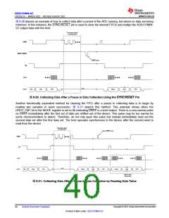
8.5.1.5 Data Ready (DRDY)
The DRDY pin is an active low output that indicates when new conversion data are ready in conversion mode or
that the requirements are met for current detection when in current-detect mode. Connect the DRDY pin to a
digital input on the host to trigger periodic data retrieval in conversion mode.
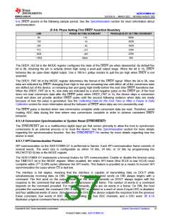
The timing of DRDY with respect to the sampling of a given channel on the ADS131M04-Q1 depends on the
phase calibration setting of the channel and the state of the DRDY_SEL[1:0] bits in the MODE register. Setting
the DRDY_SEL[1:0] bits to 00b configures DRDY to assert when the channel with the largest positive phase
calibration setting, or the most lagging, has a new conversion result. When the bits are 01b, the device asserts
DRDY each time any channel data are ready. Finally, setting the bits to either 10b or 11b configures the device to
assert DRDY when the channel with the most negative phase calibration setting, or the most leading, has new
conversion data. Changing the DRDY_SEL[1:0] bits has no effect on DRDY behavior in global-chop mode
because phase calibration is automatically disabled in global-chop mode.
The timing of the first DRDY assertion after channels are enabled or after a synchronization pulse is provided
depends on the phase calibration setting. If the channel that causes DRDY to assert has a phase calibration
setting less than zero, the first DRDY assertion can be less than one sample period from the channel being
enabled or the occurrence of the synchronization pulse. However, DRDY asserts in the next sample period if the
phase setting puts the output timing too close to the beginning of the sample period.
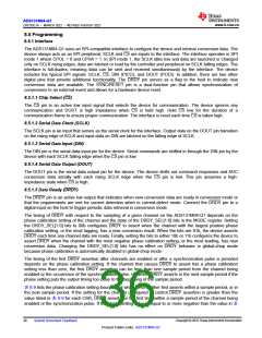
表8-9 lists the phase calibration setting boundary at which DRDY either first asserts within a sample period, or in
the next sample period. If the setting for the channel configured to control DRDY assertion is greater than the
value listed in 表 8-9 for each OSR, DRDY asserts for the first time within a sample period of the channel being
enabled or the synchronization pulse. If the phase setting value is equal to or more negative than the value in 表
Copyright © 2022 Texas Instruments Incorporated
36
Submit Document Feedback
Product Folder Links: ADS131M04-Q1

 TI [ TEXAS INSTRUMENTS ]