ADS131M04-Q1
ZHCSOL7A –MARCH 2022 –REVISED AUGUST 2022
www.ti.com.cn
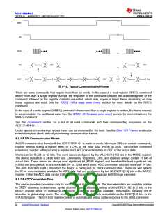
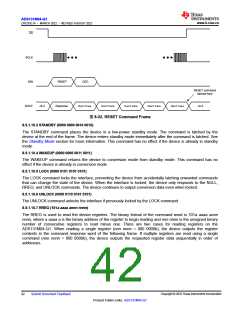
DRDY
CS
SCLK
DIN
Command
CRC
Command
CRC
DOUT
Hi-Z
Response
Channel 0 Data Channel 1 Data Channel 2 Data Channel 3 Data
CRC
Hi-Z
Response
Channel 0 Data
图8-18. Typical Communication Frame
There are some commands that require more than six words. In the case of a read register (RREG) command
where more than a single register is read, the response to the command contains the acknowledgment of the
command followed by the register contents requested, which may require a larger frame depending on how
many registers are read. See the RREG (101a aaaa annn nnnn) section for more details on the RREG
command.
In the case of a write register (WREG) command where more than a single register is written, the frame extends
to accommodate the additional data. See the WREG (011a aaaa annn nnnn) section for more details on the
WREG command.
See the Commands section for a list of all valid commands and their corresponding responses on the
ADS131M04-Q1.
Under special circumstances, a data frame can be shortened by the host. See the Short SPI Frames section for
more information about artificially shortening communication frames.
8.5.1.8 SPI Communication Words
An SPI communication frame with the ADS131M04-Q1 is made of words. Words on DIN can contain commands,
register settings during a register write, or a CRC of the input data. Words on DOUT can contain command
responses, register settings during a register read, ADC conversion data, or CRC of the output data.
Words can be 16, 24, or 32 bits. The word size is configured by the WLENGTH[1:0] bits in the MODE register.
The device defaults to a 24-bit word size. Commands, responses, CRC, and registers always contain 16 bits of
actual data. These words are always most significant bit (MSB) aligned, and therefore the least significant bits
(LSBs) are zero-padded to accommodate 24- or 32-bit word sizes. ADC conversion data are nominally 24 bits.
The ADC truncates eight LSBs when the device is configured for 16-bit communication. There are two options
for 32-bit communication available for ADC data that are configured by the WLENGTH[1:0] bits in the MODE
register. Either the ADC data can be LSB padded with zeros or the data can be MSB sign extended.
8.5.1.9 ADC Conversion Data
The device provides conversion data for each channel at the data rate. The time when data are available relative
to DRDY asserting is determined by the channel phase calibration setting and the DRDY_SEL[1:0] bits in the
MODE register when in continuous-conversion mode. All data are available immediately following DRDY
assertion in global-chop mode. The conversion status of all channels is available as the DRDY[3:0] bits in the
STATUS register. The STATUS register content is automatically output as the response to the NULL command.
Copyright © 2022 Texas Instruments Incorporated
38
Submit Document Feedback
Product Folder Links: ADS131M04-Q1

 TI [ TEXAS INSTRUMENTS ]