ADS131M04-Q1
ZHCSOL7A –MARCH 2022 –REVISED AUGUST 2022
www.ti.com.cn
8.4 Device Functional Modes
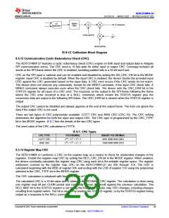
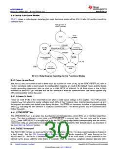
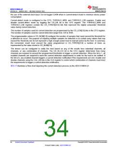
图 8-13 shows a state diagram depicting the major functional modes of the ADS131M04-Q1 and the transitions
between them.
POR, pin reset, or
RESET command
Reset
complete
Reset
STANDBY
Standby
Mode
Continuous
Conversion Mode
WAKEUP && GC_EN
STANDBY
Current detection
complete
GC_EN
WAKEUP
&& GC_EN
GC_EN
Current
Detect Mode
Global-Chop
Mode
SYNC
图8-13. State Diagram Depicting Device Functional Modes
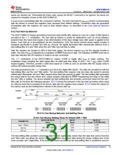
8.4.1 Power-Up and Reset
The ADS131M04-Q1 is reset in one of three ways: by a power-on reset (POR), by the SYNC/RESET pin, or by a
RESET command. After a reset occurs, the configuration registers are reset to the default values and the device
begins generating conversion data as soon as a valid MCLK is provided. In all three cases a low to high
transition on the DRDY pin indicates that the SPI interface is ready for communication. The device ignores any
SPI communication before this point.
8.4.1.1 Power-On Reset
Power-on reset (POR) is the reset that occurs when a valid supply voltage is first applied. The POR process
requires tPOR from when the supply voltages reach 90% of their nominal value. Internal circuitry powers up and
the registers are set to their default state during this time. The DRDY pin transitions from low to high immediately
after tPOR indicating the SPI interface is ready for communication. The device ignores any SPI communication
before this point.
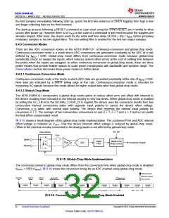
8.4.1.2 SYNC/RESET Pin
The SYNC/RESET pin is an active low, dual-function pin that generates a reset if the pin is held low longer than
tw(RSL). The device maintains a reset state until SYNC/RESET is returned high. The host must wait for at least
tREGACQ after SYNC/RESET is brought high or for the DRDY rising edge before communicating with the device.
Conversion data are generated immediately after the registers are reset to their default values, as described in
the Fast Start-Up Behavior section.
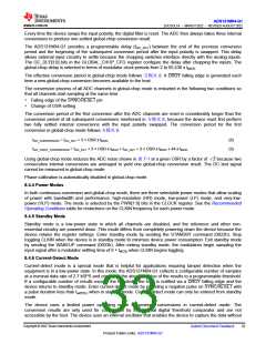
8.4.1.3 RESET Command
The ADS131M04-Q1 can be reset via the SPI RESET command (0011h). The device communicates in frames of
a fixed length. See the SPI Communication Frames section for details regarding SPI data framing on the
ADS131M04-Q1. The RESET command occurs in the first word of the data frame, but the command is not
latched by the device until the entire frame is complete. After the response completes channel data and CRC
Copyright © 2022 Texas Instruments Incorporated
30
Submit Document Feedback
Product Folder Links: ADS131M04-Q1

 TI [ TEXAS INSTRUMENTS ]