ADS131M04-Q1
ZHCSOL7A –MARCH 2022 –REVISED AUGUST 2022
www.ti.com.cn
ûꢀ
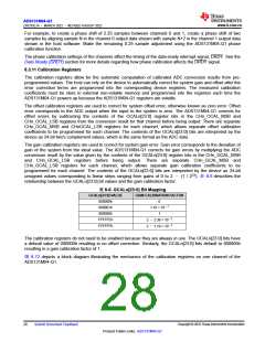
Modulator
Digital
Filter
To Interface
Å
1
223
OCALn[23:0]
GCALn[23:0]
图8-12. Calibration Block Diagram
8.3.12 Communication Cyclic Redundancy Check (CRC)
The ADS131M04-Q1 features a cyclic redundancy check (CRC) engine on both input and output data to mitigate
SPI communication errors. The CRC word is 16 bits wide for either input or output CRC. Coverage includes all
words in the SPI frame where the CRC is enabled, including padded bits in a 32-bit word size.
CRC on the SPI input is optional and can be enabled and disabled by writing the RX_CRC_EN bit in the MODE
register. Input CRC is disabled by default. When the input CRC is enabled, the device checks the provided input
CRC against the CRC generated based on the input data. A CRC error occurs if the CRC words do not match.
The device does not execute any commands, except for the WREG command, if the input CRC check fails. A
WREG command always executes even when the CRC check fails. The device sets the CRC_ERR bit in the
STATUS register for all cases of a CRC error. The response on the output in the SPI frame following the frame
where the CRC error occurred is that of a NULL command, which means the STATUS register plus the
conversion data are output in the following SPI frame. The CRC_ERR bit is cleared when the STATUS register is
output.
The output CRC cannot be disabled and always appears at the end of the output frame. The host can ignore the
data if the output CRC is not used.
There are two types of CRC polynomials available: CCITT CRC and ANSI CRC (CRC-16). The CRC setting
determines the algorithm for both the input and output CRC. The CRC type is programmed by the CRC_TYPE
bit in the MODE register. 表8-7 lists the details of the two CRC types.
The seed value of the CRC calculation is FFFFh.
表8-7. CRC Types
CRC TYPE
CCITT CRC
ANSI CRC
POLYNOMIAL
x16 + x12 + x5 + 1
x16 + x15 + x2 + 1
BINARY POLYNOMIAL
0001 0000 0010 0001
1000 0000 0000 0101
8.3.13 Register Map CRC
The ADS131M04-Q1 performs a CRC on the register map as a means to check for unintended changes to the
registers. Enable the register map CRC by setting the REG_CRC_EN bit in the MODE register. When enabled,
the device constantly calculates the register map CRC using each bit in the writable register space. The register
addresses covered by the register map CRC on the ADS131M04-Q1 are 02h through 1Ch. The CRC is
calculated beginning with the MSB of register 02h and ending with the LSB of register 1Ch using the polynomial
selected in the CRC_TYPE bit in the MODE register.
The CRC calculation is initialized with the seed value of FFFFh.
The calculated CRC is a 16-bit value and is stored in the REGMAP_CRC register. The calculation is done using
one register map bit per CLKIN period and constantly checks the result against the previous calculation. The
REG_MAP bit in the STATUS register is set to flag the host if the register map CRC changes, including changes
resulting from register writes. The bit is cleared by reading the STATUS register, or by the STATUS register being
output as a response to the NULL command.
Copyright © 2022 Texas Instruments Incorporated
Submit Document Feedback
29
Product Folder Links: ADS131M04-Q1

 TI [ TEXAS INSTRUMENTS ]