ADS131M04-Q1
ZHCSOL7A –MARCH 2022 –REVISED AUGUST 2022
www.ti.com.cn
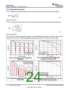
For example, to create a phase shift of 2.25 samples between channels 0 and 1, create a phase shift of two
samples by aligning sample N in the channel 0 output data stream with sample N+2 in the channel 1 output data
stream in the host software. Make the remaining 0.25 sample adjustment using the ADS131M04-Q1 phase
calibration function.
The phase calibration settings of the channels affect the timing of the data-ready interrupt signal, DRDY. See the
Data Ready (DRDY) section for more details regarding how phase calibration affects the DRDY signal.
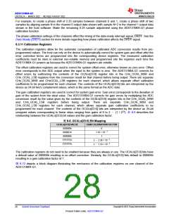
8.3.11 Calibration Registers
The calibration registers allow for the automatic computation of calibrated ADC conversion results from pre-
programmed values. The host can rely on the device to automatically correct for system gain and offset after the
error correction terms are programmed into the corresponding device registers. The measured calibration
coefficients must be store in external non-volatile memory and programmed into the registers each time the
ADS131M04-Q1 powers up because the ADS131M04-Q1 registers are volatile.
The offset calibration registers are used to correct for system offset error, otherwise known as zero error. Offset
error corresponds to the ADC output when the input to the system is zero. The ADS131M04-Q1 corrects for
offset errors by subtracting the contents of the OCALn[23:0] register bits in the CHn_OCAL_MSB and
CHn_OCAL_LSB registers from the conversion result for that channel before being output. There are separate
CHn_OCAL_MSB and CHnOCAL_LSB registers for each channel, which allows separate offset calibration
coefficients to be programmed for each channel. The contents of the OCALn[23:0] bits are interpreted by the
device as 24-bit two's complement values, which is the same format as the ADC data.
The gain calibration registers are used to correct for system gain error. Gain error corresponds to the deviation of
gain of the system from the ideal value. The ADS131M04-Q1 corrects for gain errors by multiplying the ADC
conversion result by the value given by the contents of the GCALn[23:0] register bits in the CHn_GCAL_MSB
and CHn_GCAL_LSB registers before being output. There are separate CHn_GCAL_MSB and
CHn_GCAL_LSB registers for each channel, which allows separate gain calibration coefficients to be
programmed for each channel. The contents of the GCALn[23:0] bits are interpreted by the device as 24-bit
unsigned values corresponding to linear steps ranging from gains of 0 to 2 – (1 / 223). 表 8-6 describes the
relationship between the GCALn[23:0] bit values and the gain calibration factor.
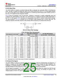
表8-6. GCALn[23:0] Bit Mapping
GCALn[23:0] VALUE
GAIN CALIBRATION FACTOR
000000h
0
000001h
1.19 × 10⁻⁷
800000h
1
2 –2.38 × 10⁻⁷
2 –1.19 × 10⁻⁷
FFFFFEh
FFFFFFh
The calibration registers do not need to be enabled because they are always in use. The OCALn[23:0] bits have
a default value of 000000h resulting in no offset correction. Similarly, the GCALn[23:0] bits default to 800000h
resulting in a gain calibration factor of 1.
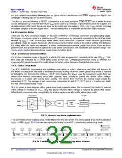
图 8-12 depicts a block diagram illustrating the mechanics of the calibration registers on one channel of the
ADS131M04-Q1.
Copyright © 2022 Texas Instruments Incorporated
28
Submit Document Feedback
Product Folder Links: ADS131M04-Q1

 TI [ TEXAS INSTRUMENTS ]