ADS131M04-Q1
ZHCSOL7A –MARCH 2022 –REVISED AUGUST 2022
www.ti.com.cn
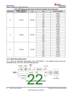
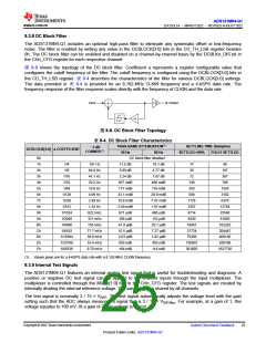
8.3.8 DC Block Filter
The ADS131M04-Q1 includes an optional high-pass filter to eliminate any systematic offset or low-frequency
noise. The filter is enabled by writing any value in the DCBLOCK[3:0] bits in the CD_TH_LSB register besides
0h. The DC block filter can be enabled and disabled on a channel-by-channel basis by the DCBLKn_DIS bit in
the CHn_CFG register for each respective channel.
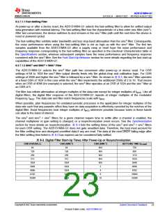
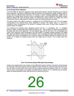
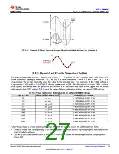
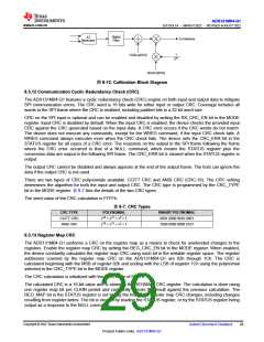
图 8-8 shows the topology of the DC block filter. Coefficient a represents a register configurable value that
configures the cutoff frequency of the filter. The cutoff frequency is configured using the DCBLOCK[3:0] bits in
the CD_TH_LSB register. 表 8-4 describes the characteristics of the filter for various DCBLOCK[3:0] settings.
The data provided in 表 8-4 is provided for an 8.192-MHz CLKIN frequency and a 4-kSPS data rate. The
frequency response of the filter response scales directly with the frequency of CLKIN and the data rate.
a
2
1Å
Input
Output
z-1
1-z-1
Åa
图8-8. DC Block Filter Topology
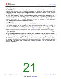
表8-4. DC Block Filter Characteristics
PASS-BAND ATTENUATION(1)
SETTLING TIME (Samples)
SETTLED >99% FULLY SETTLED
–3-dB
DCBLOCK[3:0] a COEFFICIENT
CORNER(1)
50 Hz
60 Hz
0h
DC block filter disabled
1h
2h
3h
4h
5h
6h
7h
8h
9h
Ah
Bh
Ch
Dh
Eh
Fh
1/4
1/8
181 Hz
84.8 Hz
11.5 dB
10.1 dB
4.77 dB
17
88
5.89 dB
2.24 dB
36
72
187
387
1/16
41.1 Hz
1.67 dB
1/32
20.2 Hz
657 mdB
171 mdB
43.1 mdB
10.8 mdB
2.69 mdB
671 µdB
168 µdB
41.9 µdB
10.5 µdB
2.63 µdB
655 ndB
164 ndB
466 mdB
119 mdB
29.9 mdB
7.47 mdB
1.87 mdB
466 µdB
116 µdB
29.1 µdB
7.27 µdB
1.82 µdB
455 ndB
114 ndB
146
786
1/64
10.0 Hz
293
1585
1/128
1/256
1/512
1/1024
1/2048
1/4096
1/8192
1/16384
1/32768
1/65536
4.99 Hz
588
3182
2.49 Hz
1178
2357
4714
9430
18861
37724
75450
150901
301803
6376
1.24 Hz
12764
25540
51093
102202
204447
409156
820188
1627730
622 mHz
311 mHz
155 mHz
77.7 mHz
38.9 mHz
19.4 mHz
9.70 mHz
(1) Values given are for a 4-kSPS data rate with a 8.192-MHz CLKIN frequency.
8.3.9 Internal Test Signals
The ADS131M04-Q1 features an internal analog test signal that is useful for troubleshooting and diagnosis. A
positive or negative DC test signal can be applied to the channel inputs through the input multiplexer. The
multiplexer is controlled through the MUXn[1:0] bits in the CHn_CFG register. The test signals are created by
internally dividing the internal reference voltage. The same signal is shared by all channels.
The test signal is nominally 2 / 15 × VREF. The test signal automatically adjusts the voltage level with the gain
setting such that the ADC always measures a signal that is 2 / 15 × VDiff Max. For example, at a gain of 1, this
voltage equates to 160 mV. At a gain of 2, this voltage is 80 mV.
Copyright © 2022 Texas Instruments Incorporated
Submit Document Feedback
25
Product Folder Links: ADS131M04-Q1

 TI [ TEXAS INSTRUMENTS ]