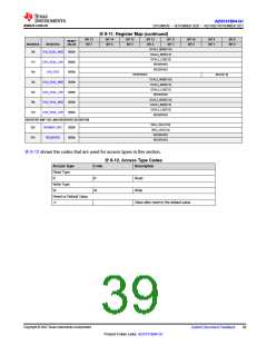
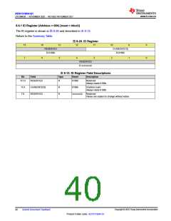
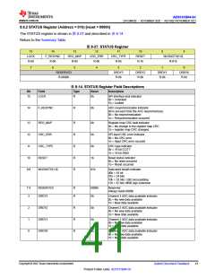
ADS131B04-Q1
ZHCSMK3B –NOVEMBER 2020 –REVISED NOVEMBER 2021
www.ti.com.cn
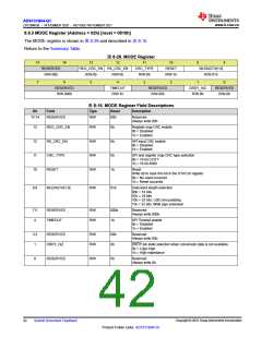
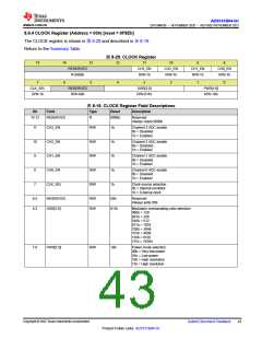
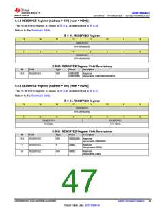
8.6.4 CLOCK Register (Address = 03h) [reset = 0F8Eh]
The CLOCK register is shown in 图8-29 and described in 表8-16.
Return to the Summary Table.
图8-29. CLOCK Register
15
14
13
12
11
10
9
8
RESERVED
R-0000b
CH3_EN
R/W-1b
CH2_EN
R/W-1b
CH1_EN
R/W-1b
CH0_EN
R/W-1b
7
6
5
4
3
2
1
0
CLK_SEL
R/W-1b
RESERVED
R/W-00b
OSR[2:0]
R/W-011b
PWR[1:0]
R/W-10b
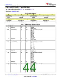
表8-16. CLOCK Register Field Descriptions
Bit
Field
Type
Reset
Description
15:12
RESERVED
R
0000b
Reserved
Always reads 0000b
11
10
9
CH3_EN
R/W
R/W
R/W
R/W
R/W
1b
1b
1b
1b
1b
Channel 3 ADC enable
0b = Disabled
1b = Enabled
CH2_EN
CH1_EN
CH0_EN
CLK_SEL
Channel 2 ADC enable
0b = Disabled
1b = Enabled
Channel 1 ADC enable
0b = Disabled
1b = Enabled
8
Channel 0 ADC enable
0b = Disabled
1b = Enabled
7
Clock source selection
0b = Internal oscillator
1b = External clock
6:5
4:2
RESERVED
OSR[2:0]
R/W
R/W
00b
Reserved
Always write 00b
011b
Modulator oversampling ratio selection
000b = 128
001b = 256
010b = 512
011b = 1024
100b = 2048
101b = 4096
110b = 8192
111b = 16384
1:0
PWR[1:0]
R/W
10b
Power mode selection
00b = Very-low power
01b = Low power
10b = High resolution
11b = High resolution
Copyright © 2022 Texas Instruments Incorporated
Submit Document Feedback
43
Product Folder Links: ADS131B04-Q1

 TI [ TEXAS INSTRUMENTS ]