ADS131B04-Q1
ZHCSMK3B –NOVEMBER 2020 –REVISED NOVEMBER 2021
www.ti.com.cn
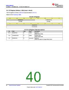
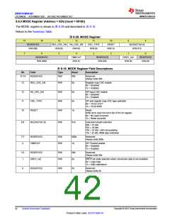
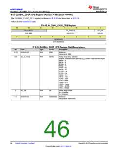
8.6.3 MODE Register (Address = 02h) [reset = 0510h]
The MODE register is shown in 图8-28 and described in 表8-15.
Return to the Summary Table.
图8-28. MODE Register
15
14
13
12
11
10
9
1
8
RESERVED
R/W-00b
REG_CRC_EN RX_CRC_EN
CRC_TYPE
R/W-0b
RESET
R/W-1b
WLENGTH[1:0]
R/W-01b
R/W-0b
5
R/W-0b
7
6
4
3
2
0
RESERVED
R/W-000b
TIMEOUT
R/W-1b
RESERVED
R/W-00b
DRDY_HiZ
R/W-0b
RESERVED
R/W-0b
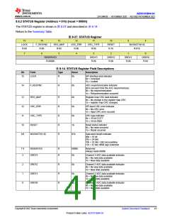
表8-15. MODE Register Field Descriptions
Bit
Field
Type
Reset
Description
15:14
RESERVED
R/W
00b
Reserved
Always write 00b
13
REG_CRC_EN
R/W
R/W
R/W
R/W
0b
0b
0b
1b
Register map CRC enable
0b = Disabled
1b = Enabled
12
11
10
RX_CRC_EN
CRC_TYPE
RESET
SPI input CRC enable
0b = Disabled
1b = Enabled
SPI and register map CRC type selection
0b = 16 bit CCITT
1b = 16 bit ANSI
Reset
Write 0b to clear this bit in the STATUS register
0b = No reset occurred
1b = Reset occurred
9:8
WLENGTH[1:0]
R/W
01b
Data word length selection
00b = 16 bits
01b = 24 bits
10b = 32 bits: LSB zero padding
11b = 32 bits: MSB sign extension
7:5
4
RESERVED
TIMEOUT
R/W
R/W
000b
1b
Reserved
Always write 000b
SPI Timeout enable
0b = Disabled
1b = Enabled
3:2
1
RESERVED
DRDY_HiZ
R/W
R/W
00b
0b
Reserved
Always write 00b
DRDY pin state selection when conversion data is not available
0b = Logic high
1b = High impedance
0
RESERVED
R/W
0b
Reserved
Always write 0b
Copyright © 2022 Texas Instruments Incorporated
42
Submit Document Feedback
Product Folder Links: ADS131B04-Q1

 TI [ TEXAS INSTRUMENTS ]