ADS131B04-Q1
ZHCSMK3B –NOVEMBER 2020 –REVISED NOVEMBER 2021
www.ti.com.cn
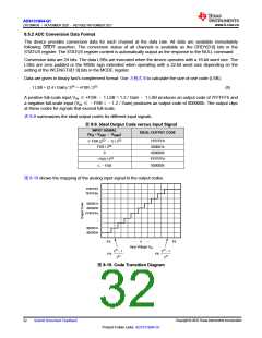
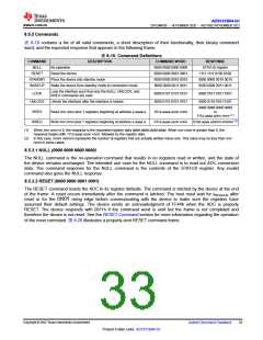
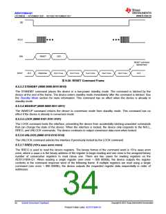
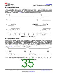
8.5.3.8 WREG (011a aaaa annn nnnn)
The WREG command allows writing an arbitrary number of contiguous device registers. The binary format of the
command word is 011a aaaa annn nnnn, where a aaaa a is the binary address of the register to begin writing
and nnn nnnn is the unsigned binary number of consecutive registers to write minus one. Send the data to be
written immediately following the command word. Write the intended contents of each register into individual
words, MSB aligned.
If the input CRC is enabled, write this CRC after the register data. The registers are written to the device as they
are shifted into DIN. Therefore, a CRC error does not prevent an erroneous value from being written to a
register. An input CRC error during a WREG command sets the CRC_ERR bit in the STATUS register.
The device ignores writes to read-only registers or to out-of-bounds addresses. Gaps in the register map
address space are still included in the parameter nnn nnnn, but are not writeable so no change is made to them.
The response to the WREG command that occurs in the following frame appears as 010a aaaa ammm mmmm
where mmm mmmm is the number of registers actually written minus one. This number can be checked by the
host against nnn nnnn to make sure the expected number of registers are written.
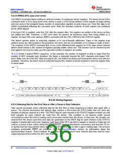
图 8-23 shows a typical WREG sequence. In this example, the number of registers to write is larger than the
number of ADC channels and, therefore, the frame is extended beyond the ADC channels and output CRC
word. Make sure all of the ADC data and output CRC are shifted out during each transaction where new data are
available. Therefore, the frame must be extended beyond the number of words required to send the register data
in some cases.
DRDY
CS
SCLK
1
st register‘s
data
2
nd register‘s
data
3
rd register‘s
data
4
th register‘s
data
5
th register‘s
data
6
th register‘s
data
N-1th register‘s
data
N
th register‘s
data
DIN
WREG
CRC
Command
CRC
DOUT
Hi-Z
Response
Channel 0 Data Channel 1 Data Channel 2 Data Channel 3 Data
CRC
Don‘t Care
Hi-Z
Response
Channel 0 Data
图8-23. Writing Registers
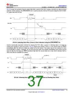
8.5.4 Collecting Data for the First Time or After a Pause in Data Collection
Take special precaution when collecting data for the first time or when beginning to collect data again after a
pause. The internal mechanism that outputs data contains a first-in-first-out (FIFO) buffer that can store two
samples of data per channel at a time. The DRDY flag for each channel in the STATUS register remains set until
both samples for each channel are read from the device. This condition is not obvious under normal
circumstances when the host is reading each consecutive sample from the device. In that case, the samples are
cleared from the device each time new data are generated so the DRDY flag for each channel in the STATUS
register is cleared with each read. However, both slots of the FIFO are full if a sample is missed or if data are not
read for a period of time. Either strobe the SYNC/RESET pin to resynchronize conversions and clear the FIFOs,
or quickly read two data packets when data are read for the first time or after a gap in reading data. This process
maintains predictable DRDY pin behavior. See the Synchronization section for information about the
synchronization feature. These methods do not need to be employed if each channel data was read for each
output data period from when the ADC was enabled.
Copyright © 2022 Texas Instruments Incorporated
36
Submit Document Feedback
Product Folder Links: ADS131B04-Q1

 TI [ TEXAS INSTRUMENTS ]