ADS131B04-Q1
ZHCSMK3B –NOVEMBER 2020 –REVISED NOVEMBER 2021
www.ti.com.cn
8.5.2 ADC Conversion Data Format
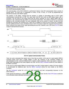
The device provides conversion data for each channel at the data rate. All data are available immediately
following DRDY assertion. The conversion status of all channels is available as the DRDY[3:0] bits in the
STATUS register. The STATUS register content is automatically output as the response to the NULL command.
Conversion data are 24 bits. The data LSBs are truncated when the device operates with a 16-bit word size. The
LSBs are zero padded or the MSBs sign extended when operating with a 32-bit word size depending on the
setting of the WLENGTH[1:0] bits in the MODE register.
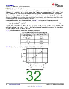
Data are given in binary two's complement format. Use 方程式8 to calculate the size of one code (LSB).
1 LSB = (2.4 / Gain) / 224 = +FSR / 223
(8)
A positive full-scale input VIN ≥+FSR –1 LSB = 1.2 / Gain –1 LSB produces an output code of 7FFFFFh and
a negative full-scale input (VIN ≤ –FSR = –1.2 / Gain) produces an output code of 800000h. The output clips
at these codes for signals that exceed full-scale.
表8-9 summarizes the ideal output codes for different input signals.
表8-9. Ideal Output Code versus Input Signal
INPUT SIGNAL
(VIN = VAINP –VAINN
IDEAL OUTPUT CODE
)
≥FSR (223 –1) / 223
FSR / 223
7FFFFFh
000001h
000000h
FFFFFFh
800000h
0
–FSR / 223
≤–FSR
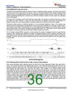
图8-19 shows the mapping of the analog input signal to the output codes.
7FFFFFh
7FFFFEh
000001h
000000h
FFFFFFh
800001h
800000h
¼
¼
-FS
-FS
0
FS
Input Voltage VIN
223 - 1
223 - 1
FS
223
223
图8-19. Code Transition Diagram
Copyright © 2022 Texas Instruments Incorporated
32
Submit Document Feedback
Product Folder Links: ADS131B04-Q1

 TI [ TEXAS INSTRUMENTS ]