ADS131B04-Q1
ZHCSMK3B –NOVEMBER 2020 –REVISED NOVEMBER 2021
www.ti.com.cn
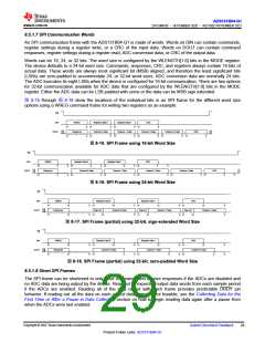
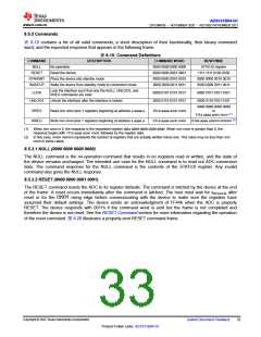
8.5.1.7 SPI Communication Words
An SPI communication frame with the ADS131B04-Q1 is made of words. Words on DIN can contain commands,
register settings during a register write, or a CRC of the input data. Words on DOUT can contain command
responses, register settings during a register read, ADC conversion data, or CRC of the output data.
Words can be 16, 24, or 32 bits. The word size is configured by the WLENGTH[1:0] bits in the MODE register.
The device defaults to a 24-bit word size. Commands, responses, CRC, and registers always contain 16 bits of
actual data. These words are always most significant bit (MSB) aligned, and therefore the least significant bits
(LSBs) are zero-padded to accommodate 24- or 32-bit word sizes. ADC conversion data are nominally 24 bits.
The ADC truncates its eight LSBs when the device is configured for 16-bit communication. There are two options
for 32-bit communication available for ADC data that are configured by the WLENGTH[1:0] bits in the MODE
register. Either the ADC data can be LSB padded with zeros or the data can be MSB sign extended.
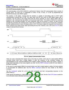
图 8-15 through 图 8-18 show the locations of the individual bits in an SPI frame for the different word size
options using a WREG command frame for writing two registers as an example.
CS
DIN
WREG
Register Data 0
Channel 0 Data
Register Data 1
Channel 1 Data
CRC
15
15
0
0
15
15
0
0
15
15
0
0
15
15
0
0
DOUT
Response
Channel 2 Data
Channel 3 Data
CRC
15
0
15
0
图8-15. SPI Frame using 16-bit Word Size
CS
DIN
WREG
Register Data 0
Register Data 1
CRC
23
23
8
8
0
0
23
23
8
0
0
23
23
8
0
0
23
23
8
0
0
DOUT
Response
Channel 0 Data
Channel 1 Data
Channel 2 Data
Channel 3 Data
CRC
23
0
23
8
0
图8-16. SPI Frame using 24-bit Word Size
CS
DIN
WREG
Register Data 0
Register Data 1
CRC
31
31
16
0
0
31
31
16
0
0
31
31
16
0
0
31
16
0
DOUT
Response
Sign ext.
Channel 0 Data
Sign ext.
Channel 1 Data
Sign ext.
31 24
Channel 2 Data
16
24
24
0
图8-17. SPI Frame (partial) using 32-bit, sign-extended Word Size
CS
DIN
WREG
Register Data 0
Register Data 1
CRC
31
31
16
16
0
0
31
31
16
Channel 0 Data
0
0
31
31
16
Channel 1 Data
0
0
31
31
16
0
0
DOUT
Response
Channel 2 Data
8
8
8
图8-18. SPI Frame (partial) using 32-bit, zero-padded Word Size
8.5.1.8 Short SPI Frames
The SPI frame can be shortened to only send commands and receive responses if the ADCs are disabled and
no ADC data are being output by the device. Read out all expected output data words from each sample period
if the ADCs are enabled. Reading all of the data output with each frame provides predictable DRDY pin
behavior. If reading out all the data on each output data period is not feasible, see the Collecting Data for the
First Time or After a Pause in Data Collection section on how to begin reading data again after a pause from
when the ADCs were last enabled.
Copyright © 2022 Texas Instruments Incorporated
Submit Document Feedback
29
Product Folder Links: ADS131B04-Q1

 TI [ TEXAS INSTRUMENTS ]