ADS131B04-Q1
ZHCSMK3B –NOVEMBER 2020 –REVISED NOVEMBER 2021
www.ti.com.cn
8.5 Programming
8.5.1 Serial Interface
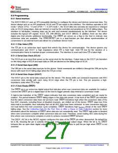
The ADS131B04-Q1 uses an SPI-compatible interface to configure the device and retrieve conversion data. The
device always acts as an SPI peripheral; SCLK and CS are inputs to the interface. The interface operates in SPI
mode 1 where CPOL = 0 and CPHA = 1. In SPI mode 1, the SCLK idles low and data are launched or changed
only on SCLK rising edges; data are latched or read by the controller and peripheral on SCLK falling edges. The
interface is full-duplex, meaning data can be sent and received simultaneously by the interface. The device
includes the typical SPI signals: SCLK, CS, DIN (MOSI), and DOUT (MISO). In addition, there are two other
digital pins that provide additional functionality. The DRDY pin serves as a flag to the host to indicate new
conversion data are available. The SYNC/RESET pin is a dual-function pin that allows synchronization of
conversions to an external event and allows for a hardware device reset.
8.5.1.1 Chip Select (CS)
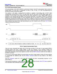
The CS pin is an active-low input signal that selects the device for communication. The device ignores any
communication and DOUT is high impedance when CS is held high. Hold CS low for the duration of a
communication frame to maintain proper communication. The interface is reset each time CS is taken high.
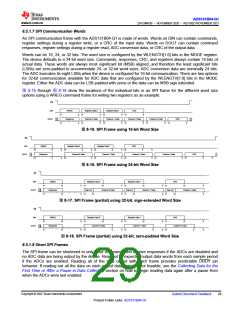
8.5.1.2 Serial Data Clock (SCLK)
The SCLK pin is an input that serves as the serial clock for the interface. Output data on the DOUT pin transition
on the rising edge of SCLK and input data on DIN are latched on the falling edge of SCLK.
8.5.1.3 Serial Data Input (DIN)
The DIN pin is the serial data input pin for the device. Serial commands are shifted in through the DIN pin by the
device with each SCLK falling edge when the CS pin is low.
8.5.1.4 Serial Data Output (DOUT)
The DOUT pin is the serial data output pin for the device. The device shifts out command responses and ADC
conversion data serially with each rising SCLK edge when the CS pin is low. This pin assumes a high-
impedance state when CS is high.
8.5.1.5 Data Ready (DRDY)
The DRDY pin is an active-low digital output that indicates when new conversion data are available for readout.
Connect the DRDY pin to a digital input on the host to trigger periodic data retrieval in conversion mode.
A high-to-low transition of the DRDY output indicates that new conversion data completed and are ready for
readout. The period between DRDY falling edges is the data-rate period. A low level of the DRDY pin indicates
that the latest conversion data have not yet been read. DRDY transitions high when the conversion data of the
four ADC channels, including those of disabled channels, are shifted out of the device. DRDY stays low if the
data read is incomplete, thus indicating that not all ADC data have been retrieved. In case conversion data are
not read before the next conversion cycle completes, DRDY transitions high tw(DRH) ahead of the next DRDY
falling edge. See the Collecting Data for the First Time or After a Pause in Data Collection section for more
information about the behavior of DRDY when data are not consistently read. The DRDY high pulse is blocked
when new conversions complete while conversion data are read. Therefore, avoid reading ADC data during the
time where new conversions complete in order to achieve consistent DRDY behavior.
The DRDY_HIZ bit in the MODE register configures the state of the DRDY pin when deasserted. By default the
bit is 0b, meaning the pin is actively driven high using a push-pull output stage. When the bit is 1b, DRDY
behaves like an open-drain digital output. Use a 100-kΩ pullup resistor to pull the pin high when DRDY is not
asserted.
Copyright © 2022 Texas Instruments Incorporated
Submit Document Feedback
27
Product Folder Links: ADS131B04-Q1

 TI [ TEXAS INSTRUMENTS ]