ADS131B04-Q1
ZHCSMK3B –NOVEMBER 2020 –REVISED NOVEMBER 2021
www.ti.com.cn
8.4.3 Conversion Modes
There are two ADC conversion modes on the ADS131B04-Q1: continuous-conversion and global-chop mode.
Continuous-conversion mode is a mode where ADC conversions are generated constantly by the ADC at a rate
defined by fMOD / OSR. Global-chop mode differs from continuous-conversion mode because global-chop
periodically chops (or swaps) the inputs, which reduces system offset errors at the cost of settling time between
the points when the inputs are swapped. In either continuous-conversion or global-chop mode, there are three
power modes that provide flexible options to scale power consumption with bandwidth and dynamic range. The
Power Modes section discusses these power modes in further detail.
8.4.3.1 Continuous-Conversion Mode
Continuous-conversion mode is the mode in which ADC data are generated constantly at the rate of fDATA
=
fMOD / OSR. New data are indicated by a DRDY falling edge at this rate. Continuous-conversion mode is
intended for measuring AC signals because this mode allows for higher output data rates than global-chop
mode.
8.4.3.2 Global-Chop Mode
The ADS131B04-Q1 incorporates a global-chop mode option to reduce offset error and offset drift inherent to the
device resulting from mismatch in the internal circuitry to very low levels. When global-chop mode is enabled by
setting the GC_EN bit in the GLOBAL_CHOP_CFG register, the device uses the conversion results from two
consecutive internal conversions taken with opposite input polarity to cancel the device offset voltage.
Conversion n is taken with normal input polarity. The device then reverses the internal input polarity for
conversion n + 1. The average of two consecutive conversions (n and n + 1, n + 1 and n + 2, and so on) yields
the final offset compensated result.
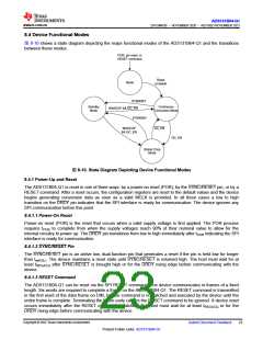
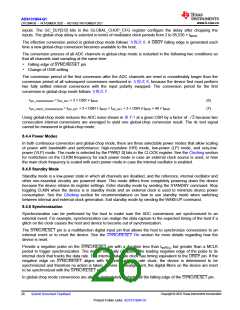
图 8-12 shows a block diagram of the global-chop mode implementation. The combined PGA and ADC internal
offset voltage is modeled as VOFS. Only this device inherent offset voltage is reduced by global-chop mode.
Offset in the external circuitry connected to the analog inputs is not affected by global-chop mode.
GC_EN
Chop Switch
VOFS
-
+
AINnP
AINnN
C
A D
Digital
Filter
Global-Chop
Mode Control
PGA
ADC
Conversion Output
图8-12. Global-Chop Mode Implementation
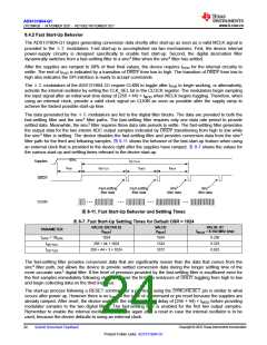
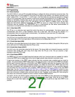
The conversion period in global-chop mode differs from the conversion time when global-chop mode is disabled
(tDATA = OSR × tMOD). 图8-13 shows the conversion timing for an ADC channel using global-chop mode.
Global-chop delay
Modulator sampling
1st global-chop
conversion result
2nd global-chop
conversion result
Conversion
start
Data not
settled
Data not
settled
Swap inputs,
digital filter reset
Data not
settled
Data not
settled
ADC overhead
Sampling
n
Sampling
n
Sampling
n
Sampling
n + 1
Sampling
n + 1
Sampling
n + 1
Sampling
n + 2
Sampling
n + 2
Sampling
n + 2
Sampling
n + 3
Sampling
n + 3
Sampling
n + 3
tGC_FIRST
tGC_CONVERSION
tDATA
CONVERSION
图8-13. Conversion Timing With Global-Chop Mode Enabled
Every time the device swaps the input polarity, the digital filter is reset. The ADC then always takes three internal
conversions to produce one settled global-chop conversion result.
The ADS131B04-Q1 provides a programmable delay (tGC_DLY) between the end of the previous conversion
period and the beginning of the subsequent conversion period after the input polarity is swapped. This delay
allows for external input circuitry to settle because the chopping switches interface directly with the analog
Copyright © 2022 Texas Instruments Incorporated
Submit Document Feedback
25
Product Folder Links: ADS131B04-Q1

 TI [ TEXAS INSTRUMENTS ]