ADS131B04-Q1
ZHCSMK3B –NOVEMBER 2020 –REVISED NOVEMBER 2021
www.ti.com.cn
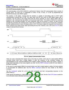
8.5.1.9 Communication Cyclic Redundancy Check (CRC)
The ADS131B04-Q1 features a cyclic redundancy check (CRC) engine on both input and output data to mitigate
SPI communication errors. The CRC word is 16 bits wide for either input or output CRC. Coverage includes all
words in the SPI frame where the CRC is enabled, including zero-padded or sign-extended bits.
CRC on the SPI input is optional and can be enabled and disabled by writing the RX_CRC_EN bit in the MODE
register. Input CRC is disabled by default. When the input CRC is enabled, the device checks the provided input
CRC against the CRC generated based on the input data. A CRC error occurs if the CRC words do not match.
The device does not execute any commands, except for the WREG command, if the input CRC check fails. A
WREG command always executes even when the CRC check fails. The device sets the CRC_ERR bit in the
STATUS register for all cases of a CRC error. The response on the output in the SPI frame following the frame
where the CRC error occurred is that of a NULL command, which means the STATUS register plus the
conversion data are output in the following SPI frame. The CRC_ERR bit is cleared when the STATUS register is
output.
The output CRC cannot be disabled and always appears at the end of the output frame. The host can ignore the
data if the output CRC is not used.
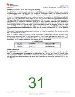
There are two types of CRC polynomials available: CCITT CRC and ANSI CRC (CRC-16). The CRC setting
determines the algorithm for both the input and output CRC. The CRC type is programmed by the CRC_TYPE
bit in the MODE register. 表 8-8 lists the details of the two CRC types. The CRC calculation is initialized with the
seed value of FFFFh to detect errors in the event that DIN or DOUT are stuck low.
表8-8. CRC Types
CRC TYPE
CCITT CRC
ANSI CRC
POLYNOMIAL
x16 + x12 + x5 + 1
x16 + x15 + x2 + 1
BINARY POLYNOMIAL
0001 0000 0010 0001
1000 0000 0000 0101
8.5.1.10 SPI Timeout
The ADS131B04-Q1 features an SPI timeout as a means to recover SPI communication, especially in situations
where CS is permanently tied low. Enable the SPI timeout using the TIMEOUT bit in the MODE register. When
enabled, the entire SPI frame (first SCLK to last SCLK) must complete in 215 MCLK cycles, otherwise the SPI
logic will reset. When a timeout happens the device starts interpreting the data starting with the next SCLK as a
new SPI frame.
Copyright © 2022 Texas Instruments Incorporated
Submit Document Feedback
31
Product Folder Links: ADS131B04-Q1

 TI [ TEXAS INSTRUMENTS ]