ADS131B04-Q1
ZHCSMK3B –NOVEMBER 2020 –REVISED NOVEMBER 2021
www.ti.com.cn
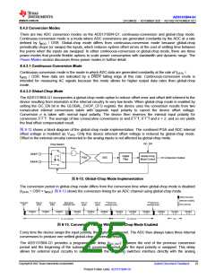
inputs. The GC_DLY[3:0] bits in the GLOBAL_CHOP_CFG register configure the delay after chopping the
inputs. The global-chop delay is selected in terms of modulator clock periods from 2 to 65,536 × tMOD
.
The effective conversion period in global-chop mode follows 方程式 6. A DRDY falling edge is generated each
time a new global-chop conversion becomes available to the host.
The conversion process of all ADC channels in global-chop mode is restarted in the following two conditions so
that all channels start sampling at the same time:
• Falling edge of SYNC/RESET pin
• Change of OSR setting
The conversion period of the first conversion after the ADC channels are reset is considerably longer than the
conversion period of all subsequent conversions mentioned in 方程式 6, because the device first must perform
two fully settled internal conversions with the input polarity swapped. The conversion period for the first
conversion in global-chop mode follows 方程式7.
tGC_CONVERSION = tGC_DLY + 3 × OSR × tMOD
(6)
(7)
tGC_FIRST_CONVERSION = tGC_DLY + 3 × OSR × tMOD + tGC_DLY + 3 × OSR x tMOD + 44 × tMOD
Using global-chop mode reduces the ADC noise shown in 表 7-1 at a given OSR by a factor of √2 because two
consecutive internal conversions are averaged to yield one global-chop conversion result. The dc test signal
cannot be measured in global-chop mode.
8.4.4 Power Modes
In both continuous-conversion and global-chop mode, there are three selectable power modes that allow scaling
of power with bandwidth and performance: high-resolution (HR) mode, low-power (LP) mode, and very-low-
power (VLP) mode. The mode is selected by the PWR[1:0] bits in the CLOCK register. See the Clocking section
for restrictions on the CLKIN frequency for each power mode in case an external clock source is used, or how
the main clock frequency is scaled with each power mode in case the internal oscillator is enabled.
8.4.5 Standby Mode
Standby mode is a low-power state in which all channels are disabled, and the reference, internal oscillator and
other non-essential circuitry are powered down. This mode differs from completely powering down the device
because the device retains its register settings. Enter standby mode by sending the STANDBY command. Stop
toggling CLKIN when the device is in standby mode and an external clock is used to minimize device power
consumption. See the Clocking section for recommendations on how to use standby mode when switching
between internal and external clock generation. Exit standby mode by sending the WAKEUP command.
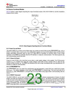
8.4.6 Synchronization
Synchronization can be performed by the host to make sure the ADC conversions are synchronized to an
external event. For example, synchronization can realign the data capture to the expected timing of the host if a
glitch on the clock causes the host and device to become out of synchronization.
The SYNC/RESET pin is a multifunction digital input pin that allows the host to synchronize conversions to an
external event or to reset the device. See the SYNC/RESET Pin section for more details regarding how the
device is reset.
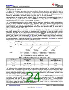
Provide a negative pulse on the SYNC/RESET pin with a duration less than tw(RSL) but greater than a MCLK
period to trigger synchronization. The device internally compares the leading negative edge of the pulse to its
internal clock that tracks the data rate. The internal data rate clock has timing equivalent to the DRDY pin. If the
negative edge on SYNC/RESET aligns with the internal data rate clock, the device is determined to be
synchronized and therefore no action is taken. If there is misalignment, the digital filters on the device are reset
to be synchronized with the SYNC/RESET pulse.
In global-chop mode conversions are always immediately restarted at the falling edge of the SYNC/RESET pin.
Copyright © 2022 Texas Instruments Incorporated
26
Submit Document Feedback
Product Folder Links: ADS131B04-Q1

 TI [ TEXAS INSTRUMENTS ]