ADS1291
ADS1292
ADS1292R
SBAS502A –DECEMBER 2011–REVISED MARCH 2012
www.ti.com
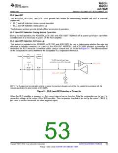
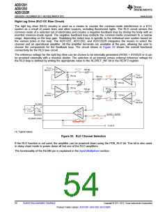
Right Leg Drive (RLD DC Bias Circuit)
The right leg drive (RLD) circuitry is used as a means to counter the common-mode interference in a ECG
system as a result of power lines and other sources, including fluorescent lights. The RLD circuit senses the
common-mode of a selected set of electrodes and creates a negative feedback loop by driving the body with an
inverted common-mode signal. The negative feedback loop restricts the common-mode movement to a narrow
range, depending on the loop gain. Stabilizing the entire loop is specific to the individual user system based on
the various poles in the loop. The ADS1291, ADS1292, and ADS1292R integrates the muxes to select the
channel and an operational amplifier. All the amplifier terminals are available at the pins, allowing the user to
choose the components for the feedback loop. The circuit shown in Figure 52 shows the overall functional
connectivity for the RLD bias circuit.
The reference voltage for the right leg drive can be chosen to be internally generated (AVDD + AVSS)/2 or it can
be provided externally with a resistive divider. The selection of an internal versus external reference voltage for
the RLD loop is defined by writing the appropriate value to the RLDREF_INT bit in the RESP2 register.
From
MUX1P
RLD1P
400 k
PGA1P
PGA1N
From
MUX2P
150 k
150 k
RLD2P
400 k
PGA2P
PGA2N
60 k
150 k
150 k
60 k
400 k
From
MUX1N
RLD1N
400 k
From
MUX2N
RLD2N
RLDINV
(1)
(1)
CEXT
1.5 nF
REXT
1 M
RLD
Amp
(AVDD + AVSS)
2
RLDOUT
RLDREF_INT
RLDIN/RLDREF
RLDREF_INT
To MUX
(1) Typical values.
Figure 52. RLD Channel Selection
If the RLD function is not used, the amplifier can be powered down using the PDB_RLD bit. This bit is also used
in daisy-chain mode to power-down all but one of the RLD amplifiers.
The functionality of the RLDIN pin is explained in the Input Multiplexer section.
54
Submit Documentation Feedback
Copyright © 2011–2012, Texas Instruments Incorporated
Product Folder Link(s): ADS1291 ADS1292 ADS1292R

 TI [ TEXAS INSTRUMENTS ]